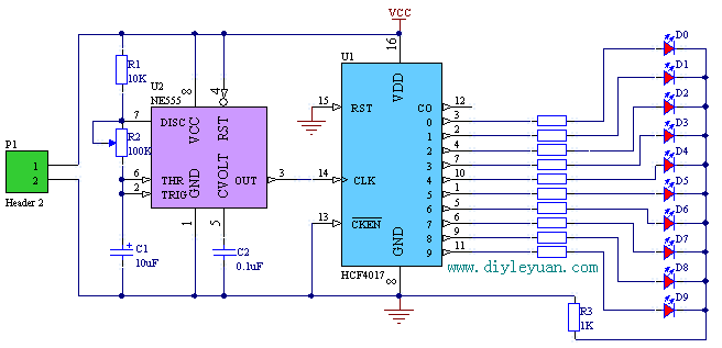
Circuit diagram of CD4017 water lamp production Circuit working principle: NE555 constitutes pulse signal generator, pulse signal is output from pin 3 of NE555 to pin 14 of CD4017. The flow rate of the water lamp can be changed by changing the resistance of R2. There are a total of 10 LEDs on the circuit. On the circuit diagram, there is a current limiting resistor for each LED. I only used one resistor during the production and PCB circuit diagram. The effect is the same. The resistance value is 1K. Various water lamp circuits can be fabricated using CD4017, which can be round, heart-shaped, and multiple LEDs combined. Readers can play freely according to this circuit. 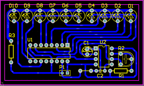
CD4017 water light PCB diagram 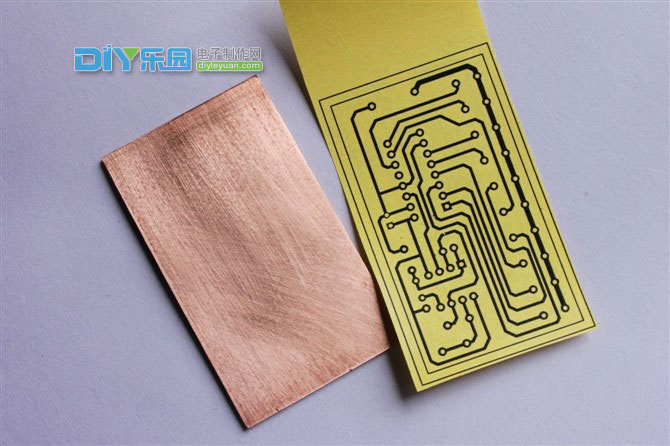
Printed thermal transfer paper and smooth the CCL 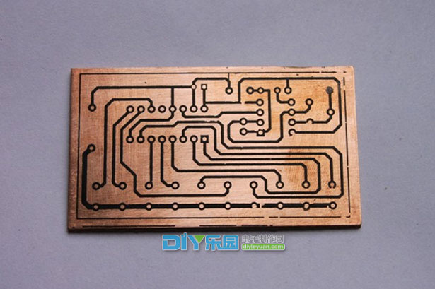
Transferred PCB wiring diagram. Repair the broken wire with an oily pen. 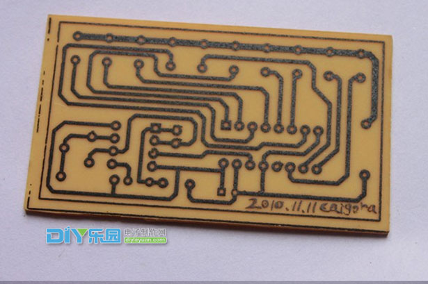
The heat-transferred PCB circuit diagram is corroded with ferric chloride. 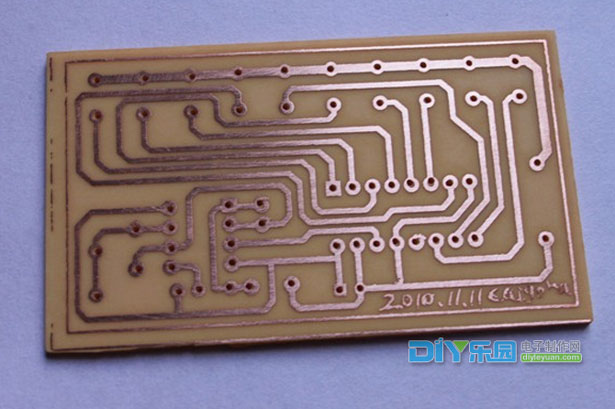
Clean the toner: Gently scrub with a fine sandpaper under the tap. 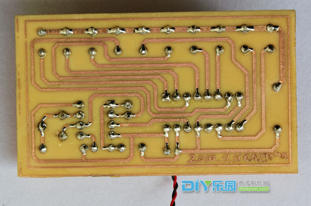
Soldered CD4017 water light circuit 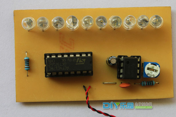
CD4017 water light circuit front photo
CBD Vape Pod
Shenzhen Xcool Vapor Technology Co.,Ltd , https://www.szxcoolvape.com