USB charger kit, also known as MP3MP4 charger, input AC160-240V, 50/60Hz, rated output: DC 5V
This article refers to the address: http://
250mA (label sticker is 500mA, if you want to output more current for a long time, please replace Q1 with 13003). MP3 and MP4 are popular in the country, but as a charger for daily use, it is directly connected with 220V high voltage, which has the characteristics of high failure rate and easy damage. Especially after buying those immature products, it is really hard to read. . Finally, commissioned by the school teacher, we contacted a mature mass-produced charger kit, which is now shared with the majority of electronic enthusiasts.
The following is a schematic diagram of the circuit drawn on the physical object: (There are a variety of component mounting methods on the Circuit Board. Please refer to the schematic and physical diagram for installation. Some component holes on the PCB should not be installed. Some components should be installed. On the component hole, please pay attention!)
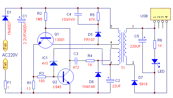
Note: In order to simplify the circuit and achieve the purpose of learning, the resistor F1 of 1 ohm acts as a fuse, and the rectification is completed by a diode D1. After the power is turned on, C1 will have a DC voltage of about 300V, and the current will be supplied to the base of Q1 through R2. The emitter of Q1 has R1 current detecting resistor R1. After the base of Q1 is energized, it will pass T1 (3, 4). Producing a collector current and simultaneously generating an induced voltage on (5, 6) (1, 2) of T1, the two secondary insulated coils of the same number of turns, wherein the T1 (1, 2) output is rectified by D7 After C5 filtering, the load is supplied to the load through the USB socket; wherein T1 (5, 6) is rectified by D6, filtered by C2, and passed through IC1 (actually 4.3V voltage regulator) and Q2 to form a sampling comparison circuit to detect the output voltage level; (5, 6), C3, R4 also form a positive feedback circuit of the Q1 transistor, so that Q1 works in high-frequency oscillation, and continuously supplies power to the T1 (3, 4) switch. When the output voltage rises due to any light load or high power supply voltage, T1 (5, 6), IC1 sampling comparison leads to Q2 conduction, Q1 base current decreases, collector current decreases, and load capacity becomes smaller. As a result, the output voltage is reduced; when the output voltage is reduced, Q2 is sampled and then turned off, Q1's load capacity becomes stronger, and the output voltage rises again; this acts as an automatic voltage regulator.
Although this circuit has few components, it is also designed with overcurrent overload and short circuit protection. When the load is overloaded or short-circuited, the collector current of Q1 increases greatly, and the emitter resistance R1 of Q1 generates a higher voltage drop. The high voltage generated by this overload or short-circuit will pass through R3 to make Q2 saturate and turn on, thus let Q1 Cut off the output to prevent overload damage. Therefore, changing the size of R1 can change the load capacity. If the required output current is small, for example, only need to output 5V100MA, the resistance of R1 can be changed. Of course, if you need to output 5V500MA, you need to change R1 appropriately. Note: R1 will increase the possibility of burning Q1. If high current output is required, it is recommended to replace the high power tube in 13003 and 13007.
What is the role of C4, R5, D5? The T1 transformer is an inductive component. Q1 operates in the switching state. When Q1 is turned off, a high voltage is induced at the collector. This voltage may be as high as 1000 volts or more, which will cause breakdown of Q1. Now there is a high-speed switching transistor. D5, this voltage can charge C4, absorb this high voltage, C4 can be discharged immediately through R5 after charging, so Q1 will not be damaged by the high voltage breakdown of the collector, therefore, if these three components have switch or damage, Q1 It is very dangerous and can be damaged in minutes and seconds.
After you receive the goods, first familiarize yourself with the circuit schematic, analyze the principle, then measure the components, and then carefully assemble.
Installation Precautions:
Please do not rush before installation. You should consult the relevant technical data and this instruction first, then follow the schematic diagram to understand the Printed Circuit Board and component list, and distinguish the components, understand the characteristics, functions and functions of each component, and check the number of components. .
Note: Z1, D2, D3, D4, IC1 This type of assembly is not equipped, the circuit board is designed for multi-purpose, this kit only uses half-wave rectification, only one 1N4007 rectification, please do not install other diodes yourself. Refer to the sample in the picture to do it, the model has been tested is OK, friends who have done in the factory know that the factory is produced according to the model.
Insert the components correctly and follow the regulations from low to high and from small to large. For manual installation, components should be installed in batches. Such a board first resistance → diode → triode → capacitor → transformer → USB seat
1, Q1, Q2 must not be wrong, Q1 should use a tube with a switching characteristic of 500V or higher, Q2 withstand voltage of several volts, Q2 is suitable for selecting tubes with good amplification characteristics, the arrangement of the two tubes May be different, please take the measurement.
2, IC1, D6 please do not install the wrong, the same is the glass package diode, a 4.3V voltage regulator diode, a common diode, where IC1 is only the symbol on the PCB board, the diode only occupies two PCB component holes.
3, 1N4007, FR107, 1N5819 please do not install the wrong, 1N4007 is a low frequency diode, FR107 is a high frequency high voltage diode, 1N5819 is a low voltage high frequency Schottky diode, can not be installed wrong position. (Substitution relationship: FR107 can replace 1N4007, but not vice versa; while 1N5819 can not be replaced by other diodes, 1N5819's turn-on voltage is very low, equivalent to the turn-on voltage of the neon tube, therefore, low voltage rectification efficiency is very high, if Be sure to replace it with other diodes, then download the output power, the heat is serious, and the efficiency is low.)
Remember: FR104(7) is a high frequency output rectifier diode, and 1N4007 is a power rectifier diode.
Power test board:
After carefully checking the circuit board installation, you can solder a 220V plug wire directly on the PCB when you want to power on the test board. For safety reasons, please connect a 10W incandescent bulb in series with the power supply to prevent short circuit or wrong connection. Pay attention to safety, and if the components are accidentally burned out, they need to be bought again. If the installation is correct, you can measure the USB with a multimeter.
The 1st and 4th feet should have a 5V voltage output, and the power indicator light is on, confirming that the board is assembled correctly.
Standard PCB
A printed circuit board (PCB) mechanically supports and electrically connects electronic components using conductive tracks, pads and other features etched from copper sheets laminated onto a non-conductive substrate. Components (e.g. capacitors, resistors or active devices) are generally soldered on the PCB. Advanced PCBs may contain components embedded in the substrate.
PCBs can be single sided (one copper layer), double sided (two copper layers) or multi-layer (outer and inner layers). Conductors on different layers are connected with vias. Multi-layer PCBs allow for much higher component density.
FR-4 glass epoxy is the primary insulating substrate. A basic building block of the PCB is an FR-4 panel with a thin layer of copper foil laminated to one or both sides. In multi-layer boards multiple layers of material are laminated together.
Printed Circuit Boards are used in all but the simplest electronic products. Alternatives to PCBs include wire wrap and point-to-point construction. PCBs require the additional design effort to lay out the circuit, but manufacturing and assembly can be automated. Manufacturing circuits with PCBs is cheaper and faster than with other wiring methods as components are mounted and wired with one single part.
Here at BentePCB, Standard PCB means manufacture parameter in General requirements, no special features.
Parameter Definition of Standard PCB as below:
|
Items |
Manufacturing Capabilities |
|
Number of Layers |
1-16 layers |
|
Material |
FR-4 |
|
Maximum PCB Size(Dimension) |
650x1200 mm |
|
Board Size Tolerance(Outline) |
±0.2mm/±0.5mm |
|
Board Thickness |
0.8-1.6mm |
|
Board Thickness Tolerance(t≥1.0mm) |
±10% |
|
Board Thickness Tolerance(t<1.0mm) |
±0.1mm |
|
Min Trace |
0.1mm/4mil |
|
Min Spacing |
|
|
Copper Thickness |
1oz(35μm) |
|
Drill Sizes (CNC) |
0.3-6.3mm |
|
Min Width of Annular Ring |
0.15mm(6mil) |
|
Finished Hole Diameter (CNC) |
0.3mm-6.2mm |
|
Finished Hole Size Tolerance(CNC) |
±0.08mm |
|
Solder Mask |
LPI |
|
Minimum Character Width(Legend) |
0.15mm |
|
Minimum Character Height (Legend) |
0.8mm |
|
Character Width to Height Ratio (Legend) |
1:05 |
|
Minimum Diameter of Plated Half Holes |
0.6mm |
|
Surface Finishing |
HASL with lead |
|
Solder Mask |
HASL lead free |
|
Immersion gold |
|
|
Green ,Red, Yellow, Blue, White ,Black |
|
|
Silkscreen |
White, Black, None |
|
Panelization |
V-scoring, |
|
|
Tab-routing, |
|
Tab-routing with Perforation (Stamp Holes) |
|
|
|
About Us:
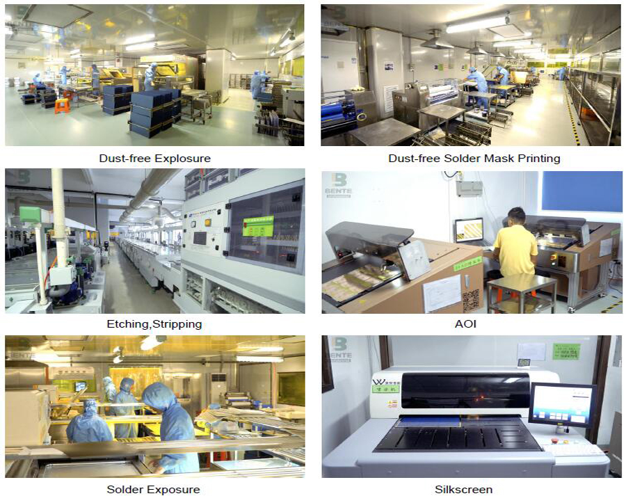
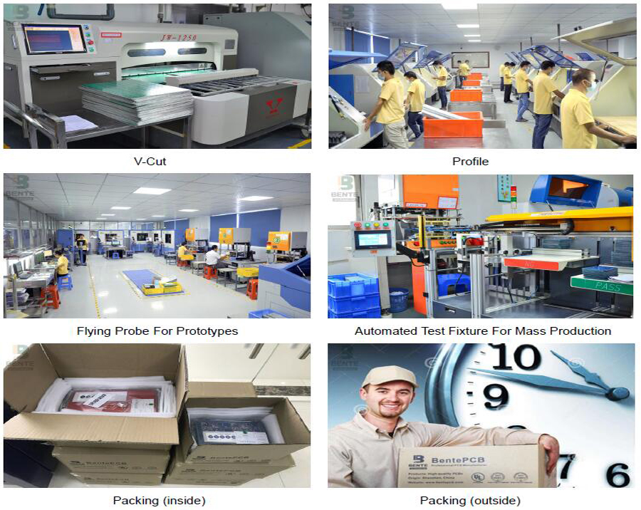
BentePCB is a professional PCB manufacturing which is focus on double side, multilayer, HDI PCB , rigid PCB and Flexible PCB mass production. The company was established on 2011.
We have two factories together, The factory in Shenzhen is specialized in small and middle volume orders and the factory in Jiangxi is for big volume.
Why Us?
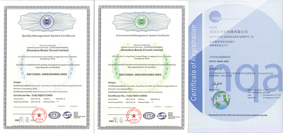
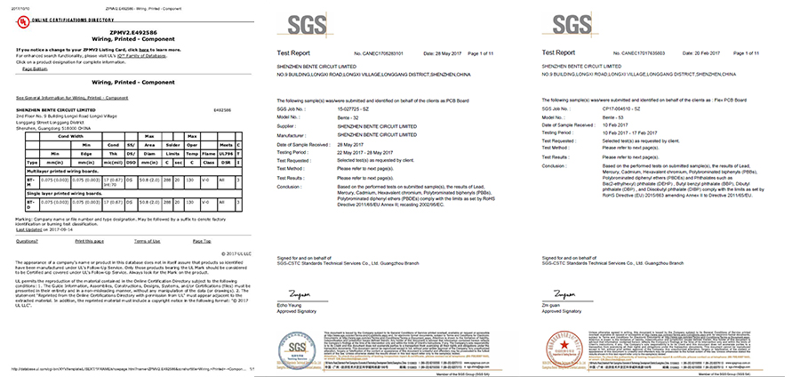
UL (E492586), ISO9001, ISO14001, TS16949, RoHS certified.
Turnover USD 10-50 million per year.
15,000 sqm area, 450 staff .
Mass Production from single to 16 layers.
Special Material:ROGERS, Arlon, Taconic.etc.
Client:Huawei, SAMSUNG, Malata, Midea,Texas Instruments.etc.
Certification(UL:E492586, TS16949, ISO14001, ISO9001,RoHS):
Factory Tour:
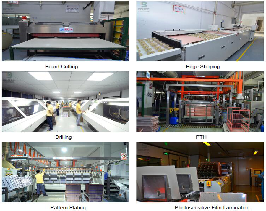
Exhibition:
We Took part in the famous exhibitions over the past years,and got highly appreciation from the top experts,as well as cooperated tightly with them.

Delivery:
BentePCB offers flexible shipping methods for our customers, you may choose from one of the methods below.


We don`t just sell PCBs .We sell sleep.

Standard PCB
Standard PCB, Printed Circuit Board, Circuit Board, PCB Circuit Board
Shenzhen Bente Circuit Limited , http://www.bentegroup.com