The RS latches, which are mutually coupled by two NAND gates [Fig. 4.2.2(a)], are the basic unit circuits of various flip-flops. They have two active-low data inputs (S(-). -): Set input; R(--: reset input) and a pair of complementary data outputs (Q and Q(--)). Q=1, when Q(--)=0, the latch is in the set state; when Q=0, Q(--)=1, the latch is in the reset state. There are four combinations of S(--) and R(--). If S(--) is invalid, R(--) is invalid, the state of the latch will be the same as the initial state; if S(--) is valid, R(--) is invalid, the state of the latch will be Q=1, Q(--)=0; if S(--) is invalid, R(--) is valid, the state of the latch will be Q= 0,Q(--)=1; If S(--) is valid and R(--) is valid, the state of the latch will be indeterminate. How to understand the last input combination? 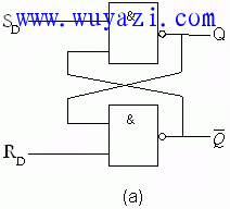
Figure 4.2.2 Basic RS Trigger (a) Circuit Structure with NAND Gate
The RS latch can (and can only) store one binary bit, either storing one or storing zeros. If we want to store 1, we add a negative pulse to the S (--) end. The so-called negative pulse is a signal that transitions from a high level to a low level and then from a low level to a high level. When S(--) transitions from high level to low level, S(--)=0, R(--)=1, Q=1, Q(--)=0, the state of the latch Is 1; when S(--) transitions from low to high, S(--)=1, R(--)=1, the state of the latch remains unchanged and remains at 1. In other words, when the negative pulse arrives, the state of the latch is one; after the negative pulse disappears, the latch maintains this state. Similarly, if we want to store 0, we add a negative pulse to the R (--) end. So, what does it mean to add negative pulses to the S (--) and R (--) terminals at the same time? Do you want to store both 1 and 0? Obviously, this kind of requirement is logically contradictory and cannot be realized. We cannot make such an unreasonable request. So how does this input combination appear? Wow! It must be interference (or noise) at work! The presence of interference may cause the latch to malfunction. If we want to store "1", we add a negative pulse P1 at the S (--) end. When P1 comes, S(--) = 0, R(--) = 1, Q = 1, Q ( --)=0. If an interference pulse P2 appears at the R (--) end before the end of P1, then 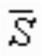
If we have S(--) =0, R(--)=0, Q=1, Q(--)=1, the problem occurs. After the problem occurs, we can analyze the three simple cases. If P2 disappears before P1, we have S(--)=0, R(--)=1, Q=1, Q(--)=0. In this case, the state of the latch is "1"; if P1 disappears earlier than P2, we will have S(--)=1, R(--)=0, Q=1, Q(-- ) = 0, in this case, the state of the latch is "0"; there is also a case where P2 and P1 disappear at the same time, we will have S (--) = 1, R (--) = 1,
Because Q=1, Q(--)=1, the input of each NAND is all “1â€. Because the transmission delay time of these two NAND gates is different, the working speed is slightly faster. The gate output rate is first "0", which will keep the output of the other NAND gate "1". Since the occurrence and disappearance of the interference pulse is random, we cannot predict which of P2 and P1 will disappear first. Due to the discrete nature of the device parameters, we also cannot predict that the NAND gate will have a shorter transmission time. Therefore, the state of the latch will be indeterminate.
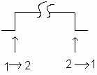
One of the uses of the RS latch is to form an "anti-jitter circuit." We know that data is usually input to a digital system via a mechanical switch. When the mechanical switch is actuated, the contacts will shake. Jitter means that the two contacts of the switch are subjected to a process that is turned on, off, re-turned on, then turned off, and reciprocated until the last turn-on. A few milliseconds of oscillation is unacceptable in digital systems. If the switch is on, it means "1", the disconnection means "0", we turn the switch on, it is expected to input a "1", but the result is a series of "1" and "0". 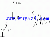
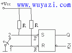
Latches or flip-flops are susceptible to interference. For example, the initial state of the RS latch is 0. If an interference pulse occurs at the S (--) terminal, the state of the latch will become "1". The strobe pulse latch [Fig. 4.2.4(a)] has a certain anti-interference ability. 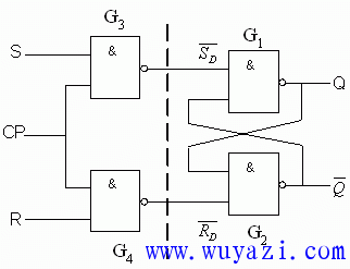
(a) Circuit structure Figure 4.2.4 Synchronous RS Trigger We see that under the control of the CP, the latch is not affected by the input signal at any time. The input signal will only work if the CP signal is "1". The CP signal is the clock signal, which is the time reference of the digital system used to coordinate (or synchronize) the actions of the various parts of the digital system. Given the importance of clock signals, designers take various measures to ensure their signal quality to avoid interference. With a data signal that is unreliable and the clock signal is relatively reliable, the use of a narrow clock pulse will significantly increase the latch's immunity to interference.
In addition to improving anti-jamming capabilities, CP signals play another role: eliminating competitive risks. If the R signal changes from 0 to 1, the S signal changes from 1 to 0. Ideally, Q and Q(--) will change simultaneously, Q will change from 1 to 0, and Q(--) will change from 0 to 1. In fact, due to the different transmission paths, there is a time difference between R and S reaching the latch. Let us assume that the S signal lags behind the R signal by Δt seconds. Thus, the latch will be in an abnormal operating state of S=1, R=1 in Δt seconds, output Q=1, Q(--)=1, such an output produces a spike in the digital system, resulting in a spike logical error. In order to eliminate this competitive risk phenomenon, we can introduce the CP signal, which causes the latch to receive the input signal for at least Δt seconds. The input signal is stable and the latch is allowed to perform logic operations. In this case, the CP signal is also called a strobe pulse.
In integrated circuit products, in addition to the RS latch, there is a D latch [Fig. 4.2.7 (a)]. 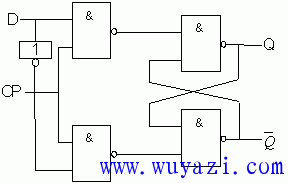
Figure 4.2.7 D-type latch circuit (a) The basic form of the pulse strobe latch has some immunity to interference. However, during CP=1, if the input signal changes multiple times, the output will also change multiple times. The master-slave flip-flop [Fig. 4.2.8(a)(b)] goes one step further than the pulse strobe latch. 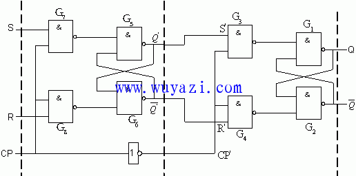
(a) 
(b)
Figure 4.2.8 Master-slave structure RS flip-flop (a) Circuit structure (b) Graphic symbol The master-slave RS flip-flop is cascaded by two pulse-gated RS latches. The CP signals of the two pulse strobe RS latches are complementary, so when the front stage receives the signal, the latter stage does not receive the signal; when the latter stage receives the signal, the pre-stage does not receive the signal. During CP=1, the front stage receives the input signal and the latter stage does not receive the input signal. If the input signal changes multiple times, the output of the previous stage (ie, the input of the latter stage) will also change several times, but the output of the latter stage will not change. At the moment when the CP changes from 1 to 0, the latter receives the input signal, and the output of the latter stage changes accordingly. However, since the pre-stage does not receive the input signal during CP=0, its output will not change any more, it will maintain the state that the CP changes from 1 to 0. Therefore, the output of the latter stage will also maintain the state of the CP from 1 to 0.
Stair Cargo Lift,Cargo Lift Elevator,Cargo Lift Installation,Home Freight Elevator
XI'AN TYPICAL ELEVATOR CO., LTD , https://www.chinaxiantypical.com