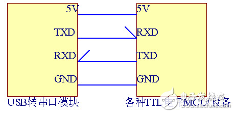
TXD: The sending end is generally expressed as its own sending end. Normal communication must be connected to the RXD of another device.
RXD: The receiving end is generally expressed as its own receiving end, and normal communication must be connected to the TXD of another device.
In normal communication, the TXD of the device is always connected to the RXD of the device!
Spontaneous: In normal communication, RXD is connected to the TXD of other devices. Therefore, if you want to receive the data you send, as you would expect, you receive the data you sent yourself. That is, your TXD is directly connected to RXD to test its own sending and receiving. Whether it is normal or not is the fastest and easiest test method. When a problem occurs, this test is first performed to determine whether the product is faulty. Also called a loopback test.
Level logic:
TTL level: Usually the data is expressed in binary, specifying +5V is equivalent to logic "1", 0V is equivalent to logic "0", called TTL signal system, is positive logic
RS232 level: -12V to -3V, equivalent to logic "0", +3V to +12V logic level, equivalent to logic "1", is negative logic.
product manual:
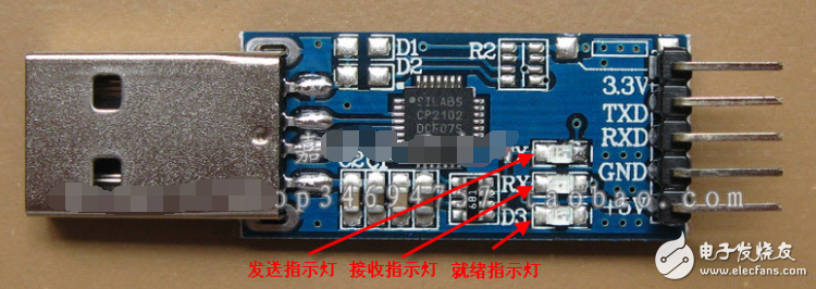
1. The main chip is CP2102. After the driver is installed, a virtual serial port is generated.
2, USB power, export interface includes 3.3V ("40mA", 5V, GND, TX, RX, signal pin level is 3.3V, positive logic
3, onboard status indicator, send and receive indicator light, after the correct installation of the driver, the status indicator will be always on, send and receive indicator light will flash in the communication, the baud rate is higher the brightness is lower
4, support baud rate from 300bps~1Mbps
5, communication format support: 1) 5,6,7,8 data bits; 2) support 1,1.5,2 stop bits; 3)odd,even,mark,space,none verification
6, support operating system: windowsvista/xp/server2003/200, MacOS-X/OS-9, Linux
7, USB head for male, can be directly connected to the computer USB port
8, SMD components for the SMT process, stable quality
9, without USB head volume: 33 * 15 (mm)
Modules and microcontrollers follow the following connections:
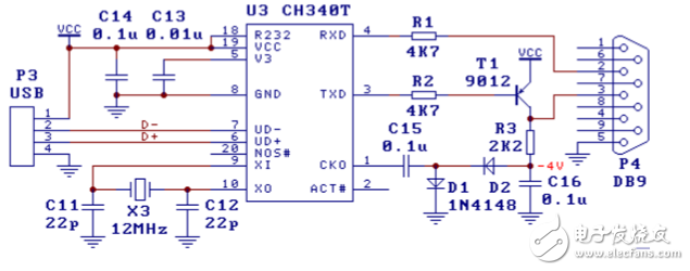
The figure is also a USB to 3-wire RS232 serial port, but the level of the output RS232 signal is slightly lower. The R232 pin of CH340 is high, and the auxiliary RS232 function is enabled. Only the diode, transistor, resistor and capacitor can be used in place of the dedicated level conversion circuit U5 in Section 7.2. Therefore, the hardware cost is lower.
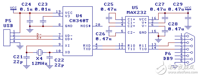
The figure shows the basic and most commonly used 3-wire RS232 serial port for USB conversion, and U5 is MAX232/ICL232/SP232.
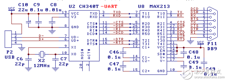
The following figure is a USB to RS232 serial port implemented by CH340T. CH340 provides commonly used serial port signals and MODEM signals. The TTL serial port is converted to an RS232 serial port through a level conversion circuit U8. Port P11 is a DB9 pin, and its pins and functions are the same as the ordinary 9-pin serial port of a computer. Similar models of U8 There are MAX213/ADM213/SP213/MAX211 and so on.
If you only need to implement USB to TTL serial port, then you can remove U8 and capacitor C46/C47/C48/C49/C40 in the figure. The signal line in the figure can be connected only to RXD, TXD, and public ground. Other signal lines can be used as needed, and can be left unconnected when they are not needed.
P2 is a USB port. The USB bus includes a pair of 5V power lines and a pair of data signal lines. Generally, the +5V power line is red, the ground line is black, the D+ signal line is green, and the D-signal line is white. The USB bus provides a maximum supply current of up to 500mA. Under normal circumstances, the CH340 chip and low-power USB products can directly use the 5V power supply provided by the USB bus. If the USB product provides the standing power through other power supply methods, the CH340 should also use the standing power supply. If you need to use the power supply of the USB bus at the same time, you can connect the 5V power cable of the USB bus and the USB product with a resistance of about 1Ω. 5V standing power supply, and the two ground lines are directly connected.
The C8 capacity is 4700pF to 0.02μF and is used to decouple the CH340 internal power supply node. The C9 capacity is 0.1μF for external power supply decoupling. Crystal X2, capacitors C6 and C7 are used for the clock oscillation circuit. X2 is a quartz crystal with a frequency of 12 MHz. C6 and C7 are monolithic or high-frequency ceramic capacitors with a capacity of 22 pF. If X2 uses a low-cost ceramic crystal, then the capacity of C6 and C7 must be recommended by the manufacturer of the crystal, which is typically 47 pF.
When designing printed circuit board PCB, it is necessary to pay attention to: Decoupling capacitors C8 and C9 should be as close as possible to the connecting pin of CH340; make D+ and D- signal lines close to parallel wiring, and try to provide grounding or copper-coating on both sides to reduce the number of The signal interference; as short as possible to reduce the length of the relevant signal line XI and XO pin, in order to reduce high-frequency interference, you can surround the ground or copper in the surrounding components.
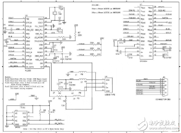
USB to serial port design principle
USB interface: mainly consists of three parts: USB connector, USB power supply, USB data transceiver, the principle is as follows:
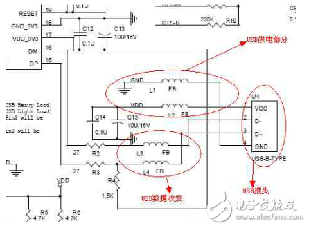
1.USB connector: Provides a USB physical interface and connects to a USB device via a USB cable.
2. USB power supply: The entire USB-to-serial cable does not require an external power supply and can be powered directly from the USB.
3. USB data transceiver: USB interface and USB to serial chip chip (PL2303) communication.
USB to serial port master chip: USB to serial port master chip module, USB to serial port master chip is the core of the circuit, providing USB and serial port bridge conversion, it consists of three parts, namely, USB to serial chip chip PL2303, PL2303 work Crystal and PL2303 peripheral circuits.
1.USB to serial main chip: USB to serial chip internal functional block diagram is as follows:
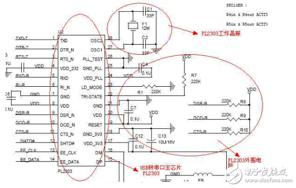
2. PL2303 working crystal: Provide PL2303 working clock, maximum support 12M frequency.
3. Peripheral circuit of PL2303: add peripheral circuit according to PL2303 data manual, see the PL2303 manual for specific peripheral circuit function.
RS232 interface: RS232 interface part realizes the conversion of serial RS232 level and TTL level. The schematic diagram of the module is as follows, mainly consists of two parts, SP232EH chip, serial port interface.
1. SP213EH chip: Convert SP2303 serial interface of TTL level into ordinary RS232 level. As well as converting ordinary RS232 level levels to TTL level serial interfaces.
2. The standard DB9 male can directly communicate data with the device.
Advantage
1. Utra Thin and Light weight, Cabinet weight only 19KG and 86mm thickness.
2. In direct sunlight, the outdoor LED Display can be high-definition and high-brightness, high refresh rate, high contrast
3. Can withstand high and low temperature, can be used in extremely harsh environment
4. Modular design, Front and Rear maintenance system available, Separate and exchangeable power and data unit can be easily removed for easy maintenance
5. Outdoor IP65 is waterproof, dustproof and corrosion proof, ensures smooth and reliable operation under variable and extreme weather conditions.
* Nova MSD 300 sending card and Nova mrv328 receiving card
* Cabinet size:640x1920mm
* Kinglight/Nationstar LED Lamp, Refresh rate:1920-3840hz
* High brightness up to 2000cd/sq.m, even in the sunlight conditions can see clear, but low power consumption to save the electric power cost.
* High debugging brightness and no damage to gray scale, achieving the debugging technology for nice image.
* Passed the TÃœV,FCC,ROHS,CE cetification.
Poster LED Display,Poster Led Display,Mirrior Led Display,Led Poster Display
Guangzhou Chengwen Photoelectric Technology co.,ltd , https://www.cwledpanel.com