Overview The DS8113 evaluation (EV) kit provides a convenient and proven platform for evaluating the DS8113. DS8113 is a low-cost, low-power analog front end for smart card readers, designed for all ISO 7816, EMV and GSM11-11 applications. DS8113 supports 5V, 3V and 1.8V smart cards, with low power consumption options for working mode and stop mode.
The DS8113 evaluation board and the attached JTAG board are shown in Figure 1. The evaluation board includes DS8113 and MAXQ2000 microcontrollers, which can be programmed to provide a complete EMV smart card interface. This interface software library function can be obtained from the CD_ROM of the kit, or download the file AN4200_sw.zip from the Maxim website for free. The evaluation board also contains a smart card slot and an LCD module with 20 characters per line for a total of two lines.
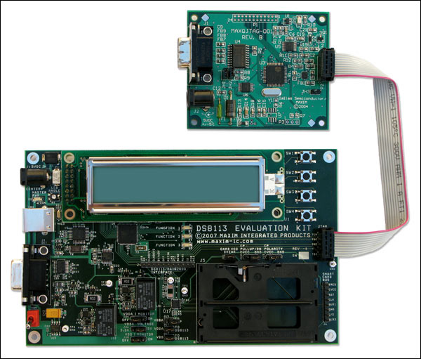
Figure 1. DS8113 evaluation board and JTAG circuit board
This application note describes how to use this evaluation kit and how to compile and run applications on this hardware platform. Three applications are provided: a simple "Hello World" program, an LCD module demonstration, and a smart card function that demonstrates actual payment terminal transactions. Provide C code for all applications.
The DS8113 device is designed to connect system microcontrollers and smart cards to provide all the power, ESD protection, and level conversion functions required for IC card applications. DS8113 is a dual power supply device. The power supply range of VDD is 2.7V to 6.0V. VDDA must be connected to 5.0V to 6.0V to provide power for the smart card. DS8113 generates smart card power supply: 1.8V, 3.0V or 5.0V. Communication with the microcontroller is achieved through the DS8113 dedicated pins and the standard input / output (I / 0) of the processor.
Software settings In this application note, Maxim's Microcontroller Toolbox (MTK), Rowley CrossWorks C language compiler and integrated development environment (IDE) are used. All software should be installed on the PC. MTK is included on the CD-ROM of the DS8113 evaluation kit or can be downloaded from the Maxim website. The Rowley toolkit can be downloaded from the website described below and has a 30-day free period of use. The steps to install these applications are as follows. If any or all of these applications have been installed in the PC, you can ignore the introduction about the installation part.
Install the microcontroller kit (MTK) Insert the CD of the DS8113 evaluation kit into the computer CD-ROM drive, the CD will automatically start and display the main interface of the DS8113 evaluation board. If the CD does not start automatically, check the CD folder and double-click the index.html file. From the main page of the CD, click the title DS8113 / MAXQ2000 EvaluaTIon Kit InformaTIon, and then click MTK. Select Run after the prompt and the installation process will begin. Follow the prompts on the screen to complete the entire process. During MTK installation, select the default settings. Note: A security warning message may appear, depending on the security settings of the website browser and the Windows® version of the computer. If a warning message appears, just confirm and continue the installation.
Install Rowley Associates' CrossWorks for MAXQ Rowley Associates provides a fully functional version of CrossWorks for MAXQ® microcontrollers with a 30-day license. The software can be downloaded from the Rowley Associates website. Follow the instructions to install. Select the default installation location and related options. Before starting the installation, you need to obtain a valid 30-day product password from Rowley Associates via email. Follow the instructions on the "Support: EvaluaTIng CrossWorks" page on the Rowley Associates website.
For more information on the setup, development, and debugging of this toolbox, please refer to application note 3698, "Getting Started with the Rowley CrossWorks and MAXQ2000 Evaluation Board."
Hardware Setup In order to load the application, some steps must be taken to configure the DS8113 evaluation board, and the evaluation board jumpers must be set correctly. The JTAG debug interface board must be connected to the evaluation board, and the serial port of the JTAG board should be connected to the PC. Finally, power on the two circuit boards. The following are the detailed steps: Configure jumpers 1 to 9 as shown in Table 1. Figure 2 shows the specific jumper locations. Note that the positions of jumpers and connector pin 1 in the figure are indicated by black circles. Connect the JTAG board and the evaluation board with the attached 10-core flat cable to ensure the correct polarity connection. On the JTAG board, when the circuit board component layer is up, the DB-9 connector is on the left and pin 1 of the JTAG connector P2 is on the lower right corner. On the evaluation board, pin 1 of the JTAG connector J2 is located in the upper left corner, as shown by the black pins in Figure 2. The side of the flat cable with red stripes should be connected to the same pin of the two circuit board JTAG connectors. Figure 1 shows the correct configuration of the two circuit boards. Connect one end of the included serial cable to the DB-9 connector J1 of the JTAG board, and the other end to the COM port of the PC. Connect the 2.5mm positive terminal of the 300mA, 5V regulated power supply (± 5%) included in the evaluation kit to the power connector J2 of the JTAG board. Make sure that the JTAG board has jumper JH3 installed to power the evaluation board from the JTAG board via the JTAG flat cable. Note that the other two jumpers (JH1 and JH2) of the JTAG board should also be installed.
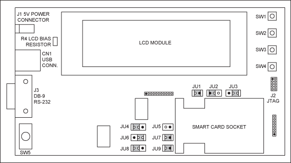
Figure 2. Jumper locations on the DS8113 circuit board
Table 1. Jumper settings for the DS8113 evaluation board
| Jumper | Installed | DescripTIon |
| JU1 | Installed | DS8113's VCC connected to smart-card socket, C1 pin |
| JU2 | Installed: connect pins 1 and 2 | DS8113's PRES pin pulled high (3.3V) through 10kΩ resistor |
| JU3 | Installed: connect pins 2 and 3 | Smart-card socket's S2 pin connected to ground |
| JU4 | Installed: connect pins 2 and 3 | Board's VDDA source connected to DS8113's VDDA pin |
| JU5 | Not Installed | DS8113's VUP pin is unused |
| JU6 | Installed: connect pins 2 and 3 | Board's 5V source selected as board's VDDA |
| JU7 | Installed | Board's VDDA source connected to DS8113's VDDA pin |
| JU8 | Installed: connect pins 2 and 3 | Board's 3.3V source selected as DS8113's VDD |
| JU9 | Installed | Board's VDD source connected to DS8113's VDD pin |
Loading an executable file can load an executable file into the 32K word (16-bit) program memory of the MAXQ2000 processor, and then run the program. Three applications written for the DS8113 evaluation kit hardware can be obtained from the kit's CD-ROM, and they are compressed into a file called an4200_sw.zip. If you do not have the CD-ROM of the kit, you can also download this file from the Maxim website. Before proceeding to the next step, a directory "\ DS8113" should be created under the C drive of the computer, and extract all the files of .ZIP to this directory. The decompressed files include source code, necessary header files, hex load files and CrossWorks project files. By placing these files in the specified directory, the software tool knows where to find the files. Otherwise, the project file needs to be updated to indicate the new location.
The first program we want to load is the "Hello World" application. In order to execute the program, there are two convenient ways to load the program from the PC to the MAXQ2000 memory: MTK and Rowley CrossWorks tool. Users can use the MTK program to load a HEX file. The quick start guide for the evaluation kit describes this method. The following will introduce how to use Rowley CrossWorks tool to load the program. Start CrossWorks MAXQ1.1 CrossStudio as described above. Click File, and then click Open Solution. Enter the C: \ DS8113 directory, select the file "HelloWorld.hzp" and open it. This will open the Hello World project. This project file contains the complete information needed by the toolbox to build the application. Make sure the JTAG board is powered up (so the DS8113 evaluation board is also powered on), and the power switch (SW5) of the evaluation board is in the ON position (the switch is facing the DB-9 connector). Right-click on the Maxim Serial JTAG Adapter option in the target window and select Connect. After connecting, the "Maxim Serial JTAG Adapter" will become bold. Click Build, and then click Build and Run. The output log at the bottom of the screen will show the progress of the program compilation. After completion, the log will indicate that the program is loaded and verified, as shown in Figure 3. Right-click Maxim Serial JTAG Adapter in the target window and select Disconnect (or click the Disconnect button). The application is loaded onto the circuit board. Remove the power supply from the JTAG and evaluation board, and disconnect the flat cable between the JTAG board and the evaluation board. CrossWorks is no longer used in the next steps, you can also close it.
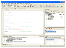
Detailed picture (PDF, 122.4kB)
Figure 3. CrossStudio screen after the "HelloWorld" project is loaded
When running the Hello World program, the HelloWorld program will send a message to the serial port, which can be received by MTK and displayed on the PC screen. Follow the steps below to run the program: Remove the RS-232 cable from the JTAG board and plug it into the DB-9 connector J3 of the DS8113 evaluation board. Find and run the MTK program. When the "Select device" window (Figure 4) appears, select Dumb Terminal and click OK. Click Options in the MTK main window, and then click Configure Serial Port. Select the PC com port (such as COM1) connected to the RS-232 cable. Select a rate of 115200 and click OK. Select Target and Open COMx at 115200 baud, where x is the com port number. Finally, connect the 5V power supply directly to J1 of the evaluation board, and switch the power switch SW5 to the DB-9 connector to supply power to the circuit board. The MTK screen will display the "Hello DS8113 World!" Message, as shown in Figure 5. Power off the circuit board through the power switch, and then power on again to reset the processor, the program will restart, and the message will be displayed again.
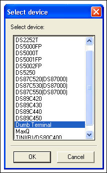
Figure 4. Select device
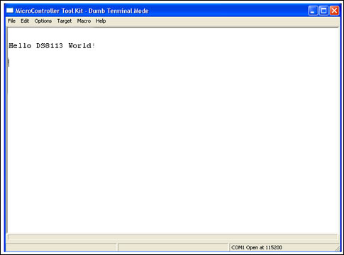
Figure 5. Output screen
Evaluation LCD display module The program running here can display information on a two-line liquid crystal display (LCD) with 20 characters per line for the evaluation kit. Before running the program, we must set the LCD contrast so that the information can be displayed correctly when the program is run. First, power up the circuit board (note that the LCD may be blank, or a black rectangular block is displayed at some character positions). Find the LCD bias resistor R4 on the circuit board (see Figure 2) and adjust the resistance with a small screwdriver until the screen shows a clear 5 x 7 dot matrix. This step will adjust the contrast of the LCD to observe clear characters, but it cannot solve the problem of blank pixels.
Follow steps 2 to 4 in the hardware setup above, and reconnect the JTAG board and power supply to the evaluation board. Follow steps 1 to 4 above to load the executable file to load the LCD demo program into the MAXQ2000 program memory. Since this application does not use a serial port, it is not necessary to follow steps 5 and 6 to disconnect the JTAG interface and RS-232 cable. In step 2, select the file LCD_8113.hzp. After completing step 4, the new demo program is loaded and starts to run. At this point, the information will be displayed on the LCD screen.
The last demo program of the smart card transaction is about the loading and running of the smart card transaction program, which realizes the basic debit operation and the smart card initialization function. Since there are no security measures related to the actual payment system, the functions demonstrated here are only a sample of the system.
The transaction routine executes and properly manages the sending and receiving of application protocol data units (APDUs) defined by the EMV specification. APDUs communicate with the ACOS3 smart card provided by the DS8113 evaluation kit. By sending the correct APDUs and processing their possible responses, the routine demonstrates a typical payment transaction process.
In order to establish a representative set of transaction functions, this example supports three main smart card operations. Debit transaction, deduct a certain amount of credit card transaction from the card balance, add a certain amount to the card amount, initialize the card transaction, set the card balance and the number of transactions to the initial value. Assume that the card has $ 100.00, and when initializing the transaction , The initial number of transactions is set to 1. To simplify this routine, whether it is a debit transaction or a credit transaction, what is deducted from or added to the card balance is a fixed amount of $ 10.00.
Follow steps 1 to 6 of the step above to load the executable file to load the smart card transaction demo program onto the evaluation board. In step 2, select the file Transaction_8113.hzp. After completing step 6, disconnect the RS-232 cable from the JTAG board and plug it into the serial port connector J3 of the evaluation board. Start the MTK program and select the device Dumb Terminal. Click Target and select Open COMx at 115200 baud, add 5V power to the circuit board, turn on the power switch (switch to DB-9 connector), and complete the expected transaction according to the instructions displayed on the LCD. The MTK screen will display the RS-232 serial port output of the program. This information can be used for analysis and debugging, or it can be ignored. However, when necessary, it can be used to analyze the application source program and determine the meaning of the serial port output.
Conclusion The DS8113 smart card interface is a low-cost analog front end for smart card readers and is designed for all applications of ISO 7816, EMV, and GSM11-11. The DS8113 supports 5V, 3V, and 1.8V smart card operation. It has low power consumption options for work mode and stop mode. The current in stop mode is as low as 10nA. The DS8113 evaluation kit provides a convenient and proven platform for evaluating the DS8113 smart card interface.
This article introduces the necessary steps for using the DS8113 evaluation board, explains software installation and configuration, hardware configuration, and the method of loading executable programs for the on-board MAXQ2000 RISC microcontroller. Provides a simple "Hello World" routine, circuit board LCD demonstration routine and actual payment system smart card transaction demonstration routine. Provide all the C program codes of the three applications, and the smart card functions are based on the EMV operation library.
360 Laptop
360 laptop sometimes is also called as Yoga Laptop , cause usually has touch screen features. Therefore you can see other names at market, like 360 flip laptop, 360 Touch Screen Laptop,360 degree rotating laptop, etc. What `s the 360 laptop price? Comparing with intel yoga laptop. Usually price is similar, but could be much cheaper if clients can accept tablet 2 In 1 Laptop with keyboard. Except yoga type, the most competitive model for Hope project or business project is that 14 inch celeron n4020 4GB 64GB Student Laptop or 15.6 inch intel celeron business laptop or Gaming Laptop. There fore, just share the basic parameters, like size, processor, memory, storage, battery, application scenarios, SSD or SSD plus HDD, two enter buttons or one is also ok, if special requirements, oem service, etc. Then can provide the most suitable solution in 1 to 2 working days. Will try our best to support you.
To make client start business more easier and extend marker much quickly, issue that only 100pcs can mark client`s logo on laptop, Mini PC , All In One PC, etc. Also can deal by insurance order to first cooperation.
360 Laptop,360 Laptop Price,360 Flip Laptop,360 Touch Screen Laptop,360 Degree Rotating Laptop
Henan Shuyi Electronics Co., Ltd. , https://www.shuyipcs.com