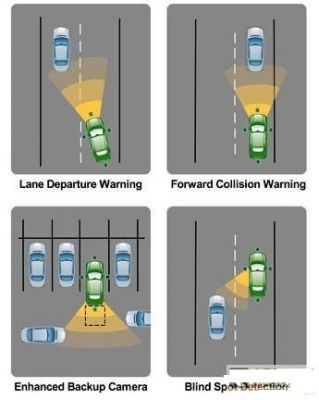
As the automotive industry continues to improve safety, vehicles need to integrate more and more peripheral photographic sensors and intelligent image processing technology to achieve advanced driver assistance systems (ADAS) such as lane departure warning, collision avoidance, blind spot monitoring, Advanced reversing photography and peripheral environment observation system with object recognition function. The common goal of manufacturers to create a completely safe driving environment is driving this trend. For example, Volvo's "Zero-by-2020" goal is that people who want to ride the new Volvo car by 2020 will no longer die or even be injured in a car accident.
This article refers to the address: http://
The challenge for these systems is the need to build a platform that maintains the processing performance required by these compute-intensive applications, consumes less power to avoid thermal issues, and provides a cost-effective solution that the integrators are willing to adopt, and the system The small size allows the system "brain" to be co-located with the image sensor and fit into the smart camera (if required). Image processing coexisting on the sensor constitutes a system solution in which the same intelligent photographic platform can be applied to different locations of the vehicle, such as the rear bumper - an enhanced reversing camera with object/human detection Mirrors - for blind spot monitoring; behind the rearview mirrors - for forward collision and lane departure warnings; and other peripheral cameras - for ambient observation. In addition, this distributed intelligent photography model does not burden the car's center console with additional processing requirements.

Figure 1: Advanced driver assistance system.
According to the market report, in the next few years, ADAS will not only be widely used in high-end cars, but also in more common medium and low-end cars. In addition to requiring more computing performance per application, there is a need to combine more ADAS applications on the same hardware platform. But it also raises a concern – is the current DSP and FPGA solution sufficient?
One of the biggest bottlenecks in DSP algorithm implementations is the burden of increasing external memory to keep up with read and write access speeds. Traditional DSPs offer limited parallel execution capabilities and typically require higher and higher frequency frequencies to meet processing requirements. As the frequency and frequency continue to rise, the DSP will consume more power, which in turn will generate more heat to be distributed. Although FPGA parallel execution capability is stronger than DSP, it is more difficult to program, and often requires RISC processor for post processing of data. FPGAs also have large power consumption, and the system size is large, in short, a costly solution.
The future of image recognition: multi-core parallel processing
The multi-core parallel processing performance performed by the CogniVue Image Recognition Processor (ICP) has surpassed DSP and FPGA in many ways. ICP can provide better cost performance in unit area and unit milliwatts of power.
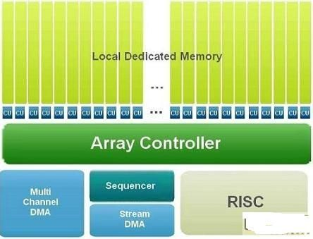
The CogniVue APEX architecture integrates an industry-standard RISC core for managing algorithm execution and a highly parallel single instruction multiple data (SIMD) array processing engine (APU) for performing low-level, computation-intensive parallel operations inherent in image processing and analysis algorithms. . In addition to RISC and APU, this architecture also has a newly designed streaming DMA to ensure efficient data movement; and a sequencer designed for automatic and efficient sorting operations to ensure maximum efficiency. The second RISC core operates independently outside of APEX and is used to handle system-level resident procedures.
The APU internally prepares local dedicated memory for each compute unit. The image data is taken from the external memory and then streamed into the APU memory. All processing is done in the APU memory before the data flows out and is stored back in the system memory. Since the APU memory and the APU unit are located in one place, the number of external memory accesses can be greatly reduced, and high computing performance can be maintained without increasing the frequency. The APEX processing core is also separate from the rest of the ICP, which means that the APEX core operating frequency is independent of the rest of the SoC, allowing the rest of the component to operate at lower frequency frequencies, saving power. By stacking the external memory inside the package, this solution can achieve a smaller system size and save board space.
With a parallel processor core and a unique software paradigm based on streaming programming, CogniVue ICP can schedule complex vector operations and execute program code with minimal data movement. These processors implement automatic pipelined operation of algorithm primitives whenever possible, and capture this complexity through a comprehensive API, thereby hiding the complexity of system load balancing and eliminating multi-core synchronization faced by developers. problem.
The highly parallel mechanism coupled with the high ALU bandwidth architecture demonstrates a viable platform that provides sufficient redundancy and processing power to execute multiple applications in parallel on the same hardware. The flexible development platform and SDK enable users to flexibly program APEX and build highly competitive and differentiated applications. This multi-core parallel platform is favored by developers not only because it provides advanced performance, power and size features, but also ensures program code reuse in future ICPs, ensuring minimal development effort and time.

Figure 2: Parallel architecture of programmable design.
Big Size Switch And Socket,Big Size Switch,Big Size Socket,Big Size Switch Socket For Sale
ZHEJIANG HUAYAN ELECTRIC CO.,LTD , https://www.huayanelectric.com