1 Introduction
The high-sensitivity satellite positioning receiver is mainly composed of an antenna, a radio frequency module, a baseband module, a pvt calculation module, and a communication and application module. As shown in Figure 1.
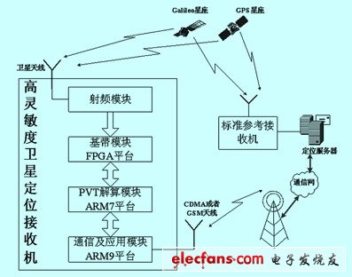
Figure 1 Receiver structure block diagram
The satellite signal (center frequency is gps, galileo l1 band 1575.42mhz) is received through the antenna (including low noise amplifier) ​​and the radio frequency module. The RF module converts the internal 16.368mhz high-precision tcxo clock through a phase-locked loop 96 times frequency to down-convert the l1 band signal to a 4.092mhz analog signal, and then samples by the 16.368mhz clock. Pass to fpga module. In order to ensure the synchronization of the positioning and solving time, the clock of 16.368mhz is used as the input clock of the fpga platform.
The baseband module fpga platform performs related arithmetic processing on the clock signal and the digital signal, and then transmits it to the pvt solving module through a high-speed bus for position resolution. The high-speed bus frequency is 66mhz.
Due to the high frequency of the above signal and as a high sensitivity receiver, the receiving sensitivity needs to reach -144dbm. The back-end communication and application module receives information data such as satellite ephemeris of the reference receiver through wireless communication and transmits the information to the pvt solution module through the serial port, which greatly improves the receiver's capture sensitivity. If the integrity of the high-speed signal is not handled properly, it will directly interfere with the front-end RF signal, thereby greatly affecting the performance of the entire receiver. In the hardware design, the reflection and crosstalk effects of the high-speed signal transmission line of the baseband part are mainly considered, and the effect is solved by stacking the PCB board and controlling the PCB line width and spacing.
2 Theoretical analysis of transmission lines
2.1 Transmission line impedance
Transmission lines are used to transmit signals from one end to the other. All transmission lines are composed of two wires of a certain length, one of which is the signal path and the other is the return path. The transmission line effect in high-speed digital circuits mainly manifests as overshoot, undershoot and ringing of digital signals. These phenomena will not only cause errors in the transmission of digital signals, but in severe cases may also damage some chips and reduce the performance of other functional modules. The root cause of these three phenomena is due to the change in the transient impedance of the signal as it travels along the interconnect. The magnitude of this type of change can be explained by the reflection coefficient.
Reflection coefficient formula (2-1)
z1 represents the transient impedance of the area where the signal is originally located, and z2 represents the transient impedance of the area where the signal enters. It can be known from equation (2-1) that when the transient impedance is the same, the reflection coefficient is 0; the greater the difference in transient impedance, the greater the reflected signal. It can be seen that, as long as the impedance of the transmission line of the entire board (ie, important high-speed signal traces) is controlled during PCB design, the signal reflection can be reduced as much as possible.
2.2 Transmission line crosstalk
Crosstalk refers to the transfer of harmful signals from one network to an adjacent network. In the PCB board, we usually route the data bus or address bus in parallel point-to-point. When these buses switch from logic high to low level, crosstalk will occur. Through superposition analysis, when the noise generated by crosstalk exceeds 15% of the signal voltage swing, it will affect the stability of the entire system. Therefore, the analysis of the allowable coupling noise between one line on the bus and another static line will become very important. The fringe field is the root cause of crosstalk. The main way to reduce crosstalk is to make the distance between the networks far enough, so that the fringe field between them can be reduced to an acceptable level. Therefore, in the PCB design, the wiring of the bus increases the line width within the range allowed by the structure, which can significantly reduce the crosstalk of the transmission line.
3 pcb board design
3.1 Power supply, ground plane analysis and stack analysis
The ground plane and stack design of the circuit board will directly affect the performance of the entire board. The high-speed signal current always advances along the path of the smallest inductance, and the return signal current tends to be near the signal conductor. The current density decreases with the square of the mutual distance increase. Therefore, the ground plane and stack design will greatly improve signal crosstalk. Consider that the whole board adopts a 10-layer board design. The specific design and settings are shown in Figure 2. For the power layer and the ground layer, the main power of the whole board is 3.3v and 1.2v, among which there are also 5v digital power, 3.3v analog power and 2.5v digital power.
3.3v is a single layer of power, and the other power layer is divided into 1.2v and 5v. 3.3v analog power supply and 2.5v digital power supply are completed through the trace layer.
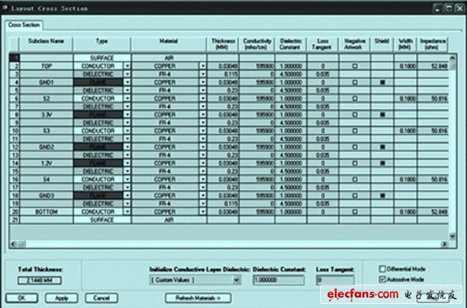
Figure 2 PCB board stacking and trace impedance matching settings
Yuchai 401-999KW Diesel Generator
Yuchai 401-999Kw Diesel Generator,Yuchai Power Generator,Yuchai Diesel Genset,Yuchai Super Silent Power Generator
Shanghai Kosta Electric Co., Ltd. , https://www.generatorksd.com