The connection between the CPU and the external device, the memory, and the data exchange are all implemented by the interface device, the former is called an I/O interface, and the latter is called a memory interface. The memory usually works under the synchronous control of the CPU. The interface circuit is relatively simple. The function of the I/O interface is responsible for implementing the CPU to link the I/O circuit and peripheral devices through the system bus. For example, SATA, which is the abbreviation of Serial ATA, is Serial ATA. This is a new type of hard disk interface that is completely different from Parallel ATA, named after the serial transfer of data. The SATA bus uses an embedded clock signal and has a stronger error correction capability. Compared with the past, the biggest difference is that it can check the transmission instructions (not just the data). If the error is found, it will be automatically corrected. This is very large. To a certain extent, the reliability of data transmission is improved. The serial interface also has the advantages of simple structure and hot swap support.
1.A[31:3]# (I/O) Address (Address Bus)
This set of address signals defines the maximum memory address space of the cpu as 4GB. In the first sub-period of the address period, these Pins transmit the address of the transaction. In the second sub-cycle of the address period, these Pins transmit the information type of the transaction.
2.A20M# (I) Adress-20 Mask (address 20 mask)
This signal is output by the ICH (South Bridge) to the cpu signal. It is to let the cpu emulate 8086 only 1M Byte (1 megabyte) address space in Real Mode. When it exceeds 1 Mbyte bit space, A20M# is Low, A20 is driven to 0 and the address is automatically folded back to the first A 1Mbyte address space.
3.ADS# (I/O) Address Strobe (address strobe)
When this signal is asserted, the data on the address signal is valid. In a new transaction, all the signals on the Bus are monitoring whether ADS# is valid. Once ADS# is valid, they will perform some corresponding actions, such as parity check, association check, address decoding and so on.
4.ADSTB[1:0]# (I/O) Address Strobes
These two signals are mainly used to lock A[31:3]# and REQ[4:0]# on their rising and falling edges. The corresponding ADSTB0# is responsible for REQ[4:0]# and A[16:3]#, and ADSTB1# is responsible for A[31:17]#.
5.AP[1:0]# (I/O) Address Parity
These two signals are primarily used for parity checking of the data on the address bus.
6.BCLK[1:0] (I) Bus Clock
These two blocks are mainly used to supply the clocks needed to make transactions on the Host Bus.
7.BNR# (I/O) Block Next Request (next request)
This signal is mainly used to declare the delay of a bus through any bus proxy, during which the owner of the current bus cannot make any new transaction.
8.BPRI# (I) Bus Priority Request
This signal is primarily used for arbitration of system bus usage rights, which must be connected to the appropriate Pin of the system bus. When BPRI# is active, all other devices stop issuing new requests unless the request is being locked. The bus owner must always keep BPRI# active until all requests are completed before releasing control of the bus.
9.BSEL[1:0] (I/O) Bus Select
These two sets of signals are mainly used to select the frequency required by the cpu. The following table defines the selected frequency:
10.D[63:0]# (I/O) Data (Data Bus)
These signal lines are the data bus that is primarily responsible for transmitting data. They provide a 64-bit channel between the cpu and the NB (Northbridge). Only when DRDY# is Low, the total online data is valid, otherwise it is regarded as invalid data.
11.DBI[3:0]# (I/O) Data Bus Inversion (Data Bus Inversion)
These signals are mainly used to indicate the polarity of the data bus. When the data of the data is always online, these signals should be Low. These four signals are each responsible for 16 data buses, as shown in the following table:
12.DBSY# (I/O) Data Bus Busy (data bus busy)
When the bus owner is using the bus, it will drive DBSY# to Low to indicate that the bus is busy. When DBSY# is High, the data bus is released.
13.DP[3:0]# (I/O) Data Parity
These four signals are mainly used to perform parity check on the data of the total data on the line.
14.DRDY# (I/O) Data Ready (data preparation)
When DRDY# is Low, it indicates that the current data of the current data is valid. If it is High, the total online data is invalid.
15.DSTBN[3:0]# (I/O) Data Strobe
Data strobe used to latch in D[63:0]# :
16.DSTBP[3:0]# (I/O) Data Strobe
Data strobe used to latch inn D[63:0]# :
17.FERR# (O) FloaTIng Point Error (floating point error)
This signal is a cpu output to the ICH (South Bridge) signal. When an unmaskable floating-point operation error occurs in the internal floating-point arithmetic unit of the CPU, FERR# is driven to be Low by cpu.
18.GTLREF (I) GTL Reference (GTL Reference Voltage)
This signal is used to set the reference voltage of the GTLn Bus. This signal is typically set to two-thirds of the Vcc voltage.
19.IGNNE# (I) Ignore Numeric Error (ignoring numeric errors)
This signal is the signal that an ICH outputs to the cpu. This signal is required to respond to the cpu when the CPU has a floating-point operation error. When IGNNE# is Low, the cpu ignores any unmaskable floating-point arithmetic errors that have occurred but have not yet been processed. However, if IGNNE# is High and there is an error, if the next floating point instruction is one of FINIT, FCLEX, FSAVE and other floating point instructions, cpu will continue to execute this floating point instruction but if the instruction is not the above instruction, cpu Will stop execution and wait for an external interrupt to handle this error.
20.INIT# (I) IniTIalizaTIon (initialization)
This signal is a signal output from the ICH to the cpu, which is very similar to the Reset function, but unlike the Reset, the internal L1 Cache and floating-point operation states of the CPU are not invalidated. However, the data in the TLB (Address Translation Reference Buffer) and BTB (Differential Address Buffer) are invalidated. Another difference between INIT# and Reset is that the CPU must wait until the space between the instruction and the instruction is confirmed, and the cpu enters the start state.
21.INTR (I) Processor Interrupt
This signal is a signal that the ICH output requests an interrupt to the CPU. When the peripheral device needs to process data, it requests an interrupt to the interrupt controller. When the CPU detects that INTR is High, the CPU first completes the bus cycle being executed, and then Only begin to process the INTR interrupt request.
22.PROCHOT# (I/O) Processor Hot (cpu over temperature indication)
When the temperature sensor of the cpu detects that the temperature of the cpu exceeds the maximum temperature set by it, the signal will become Low, and the temperature control circuit of the corresponding cpu will operate.
23.PWRGOOD (I) Power Good (power OK)
This signal is usually sent to the CPU by ICH (South Bridge) to tell the CPU that the power is OK. If this signal is not supplied to the CPU, the CPU will not be able to operate.
24.REQ[4:0]# (I/O) Command Request
These signals are connected to the NB (Northbridge) by the CPU, and when the bus owner starts a new transaction, it defines the command for the transaction.
25.RESET# (I) Reset (reset signal)
When Reset is High, the cpu is internally reset to a known state and begins reading the reset first instruction from address 0FFFFFFF0H. The internal TLB (Address Translation Reference Buffer), BTB (Differential Address Buffer), and SDC (Segment Address Translation Cache) of the CPU all become invalid when the reset occurs.
26.RS[2:0]# (I) Response Status
These signals are driven by the responder. See the table below for the specific meaning:
27.STKOCC# (O) Socket Occupied (cpu insert)
This signal is generally pulled from the cpu to the ground. The main function on the motherboard is to tell the motherboard whether the cpu is inserted for the first time. If you insert it for the first time, it will let you enter the CMOS to reset the cpu.
28.SMI# (I) System Management Interrupt
This signal is a signal output from the ICH to the CPU. When the CPU detects that SMI# is Low, it enters the SMM mode (system management mode) and reads the SMI# handler into the SMRAM (System Management RAM). In the SMM mode, the NMI, INTR, and SMI# interrupt signals are masked. It is necessary to wait until the CPU executes the RSM (Resume) command, and the SMI#, NMI, and INTR interrupt signals are recognized by the CPU.
30.STPCLK# (I) Stop Clock
When the cpu enters the power saving mode, the ICH (South Bridge) will send this signal to the CPU to let it stop its Clock.
31.TRDY# (I/O) Target Ready (target preparation)
When TRDY# is Low, it indicates that the target is ready to receive data. When it is High, Target is not ready.
32.VID[4:0] (O) Voltage ID (voltage identification)
These signals are mainly used to set the operating voltage of the cpu. These signals must be boosted to a maximum of 3V in the motherboard.
Second, VGA interface signal description1.HSYNC (O) CRT Horizontal SynchronizaTIon (horizontal sync signal)
This signal mainly provides a signal for horizontal scanning of the CRT.
2.VSYNC (O) CRT Vertical Synchronization
This signal mainly provides the signal for vertical scanning of the CRT.
3.RED (O) RED analog video output (red analog signal output)
This signal mainly provides a red primary analog video signal for the CRT.
4.GREEN (O) Green analog video output (green analog signal output)
This signal mainly provides a green primary color analog video signal for the CRT.
5.BLUE (O) Blue analog video output (blue analog signal output)
This signal mainly provides a blue primary analog video signal for the CRT.
6.REFSET (I) Resistor Set
This signal will connect a resistor to ground, primarily for the internal color palette DAC. This resistor has a resistance of 169 ohms and an accuracy of 1%.
7.DDCA_CLK (I/O) Analog DDC Clock
This signal connects NB (Northbridge) to the display. This Clock is an I眷 interface that is used in combination with DDCA_DATA to read the display's data.
8.DDCA_DATA (I/O) Analog DDC Clock
This signal is connected to the NB (North Bridge) and the display. This Data, like the Clock, is also an I眷 interface. It is used in combination with DDCA_CLK to read the data of the display.
Third, the AGP interface signal description1.GPIPE# (I/O) Pipelined Read (pipelined read)
This signal is executed by the current Master, which can be used in AGP 2.0 mode, but not in the AGP 3.0 specification. This signal is replaced by DBI_HI (Dynamic Bus Inversion HI) in the specification of AGP 3.0.
2.GSBA[7:0] (I) Sideband Address (sideband address)
This set of signals provides an additional bus to transfer addresses and commands from the AGPn Master (display card) to the GMCH (Northbridge).
3.GRBF# (I) Read Buffer Full (read buffer area full)
This signal indicates whether the Master can accept the data to be read previously requested with a low priority. When RBF# is Low, the mid-cutter will stop reading data to the Master with low priority.
4.GWBF# (I) Write Buffer Full (write buffer full)
This signal indicates whether the Master is ready to accept fast write data from the core controller. When WBF# is Low, the middle cutter will stop the transaction of this fast write data.
5.ST[2:0] (O) Status Bus
This set of signals has three BITs and can be grouped into eight groups, each of which represents the state of the current bus.
6.ADSTB0 (I/O) AD Bus Strobe 0 (Address Data Bus Gating)
This signal can provide 2X timing for AGP, which is responsible for bus AD[15:0].
7.ADSTB0# (I/O) AD Bus Strobe 0 (Address Data Bus Gating)
This signal can provide 4X timing for AGP, which is responsible for bus AD[15:0].
8.ADSTB1 (I/O) AD Bus Strobe 1 (Address Data Bus Gating)
This signal can provide 2X timing for AGP, which is responsible for bus AD[31:16].
9.ADSTB1# (I/O) AD Bus Strobe 1 (Address Data Bus Gating)
This signal can provide 4X timing for AGP, which is responsible for the line total AD[31:16].
10.SB_STB (I) SideBand Strobe (SideBand Gating)
This signal primarily provides timing for SBA[7:0], which is always driven by AGPn Master.
11.SB_STB# (I) SideBand Strobe (SideBand strobe)
This signal provides timing for SBA[7:n0] only in AGP 4X mode, which is always driven by AGP Master.
12.CLK (O) CLOCK (frequency)
Provides reference timing for AGP and PCI control signals.
13.PME# Power Management Event
This signal is not used in the AGPn protocol, but it is used by the operating system in the PCI protocol. For the detailed definition of PME#, please participate in the PCI protocol specification.
14.TYPEDET# Type Detect (Type Check)
From the perspective of AGP development, there are four modes: 1X, 2X, 4X and 8X. The voltage used in each mode is not the same. How does the AGP controller know what kind of graphics card you plugged in? It is through this signal to tell AGP Control. Use this signal to set the voltage required for the current graphics card.
15.FRAME# (I/O) Frame (Period Frame)
This signal is not used during AGP pipe transmission. This signal is only used in AGP's fast write mode.
16.IRDY# (I/O) Initiator Ready (starter ready)
This signal indicates that AGPn Master is ready for the data required for the current transaction. It is only used for write operations and AGP Master does not allow insertion of wait states.
17.TRDY# (I/O) Target Ready (target ready)
This signal indicates that AGPn Target is ready for the entire transaction to read data, this Target can be inserted into the wait state.
18.STOP# (I/O) Stop
This signal is not used when trading on AGP. For the fast write mode, when STOP# is Low, the current transaction is stopped.
19.DEVSEL# (I/O) Device Select
Not used when trading in AGP. In the fast write mode, when a transaction cannot be completed, it will be used.
20.REQ# (I) Request
This signal is used to request the current bus usage right to start a PCI orn AGP transaction.
21.GNT# (O) Grant (guaranteed)
When the middle cutter receives the request from the Initiator, if the current bus is idle, the middle cutter will pass the bus control to the Initiator through GNT#.
22.AD[31:0] (I/O) Address Data Bus
These signals are used to transfer addresses and data.
23.C/BE[3:0]# (I/O) Command/Byte Enable (Command/Byte Enable)
Provide command information when a transaction begins. Provide valid bit information when AGPn Master makes a write transaction.
Fourth, Memory interface signal description1.SCMDCLK[5:0] (O) Differential DDR Clock
SCMDCLK and SCMDCLK# are differential clock output pairs, and both the address and control signals are sampled at the intersection of the positive and negative edges of the two blocks. There are three pairs of DIMMs each.
2.SCMDCLK[5:0]# (O) Differential DDR Clock
This Clock signal has the same meaning as above.
3.SCS[3:0]# (O) Chip Select
When these signals are active, it indicates that a Chip has been selected, and each signal corresponds to one row of the SDRAM.
4.SMA[12:0] (O) Memory Address
These signals are primarily used to provide multiple row and column addresses to memory.
5.SBA[1:0] (O) Bank Address
These signals define which bank is selected in each memory bank. The Bank select signal and the memory address signal are used in conjunction with any unit that can be addressed to memory.
6.SRAS# (O) Row Address
Row address, which is used with SCAS#, SWE# to define memory commands.
7.SCAS# (O) Column Address
Column address, which is used with SRAS#, SWE# to define memory commands.
8.SWE# (O) Write Enable (write enable)
Write enable signal, which is used with SRAS#, SCAS# to define memory commands.
9.SDQ[63:0] (I/O) Data Lines
These signal lines are used to transmit data.
10.SDM[7:0] (O) Data Mask
Data transmitted in memory is masked when the write cycle is active. Each of these eight signals is responsible for eight data lines.
11.SDQS[7:0] (I/O) Data Strobe (data strobe)
These signals are primarily used to capture data. These eight signals are responsible for eight data lines per signal.
12.SCKE[3:0] (O) Clock Enable
This signal initializes the memory on power-up and they can also be used to close unused memory data lines.
Five, HUB interface signal description1.HL[10:0] (I/O) Packet Data (packet)
These signals are mainly used to transfer data when the Hub Interface reads and writes.
2.HISTRS (I/O) Packet Strobe (data strobe)
3.HISTRF (I/O) Packet Strobe Complement
This signal transmits and receives data on the HUBn inteface along with the HISTRS.
Sixth, LAN LINK interface signal description1.LAN_CLK (I) Lan I/F Clock (network clock)
This signal is driven by the Lann Chipset and has a frequency range of 5 to 50 Mhz.
2.LAN_RXD[2:0] (I) Received Data
These signals are driven by the Lan Chipset to the South Bridge. n
3.LAN_TXD[2:0] (O) Transmit Data
These signals are the south bridge drive output to the Lan Chipset. n
4.LAN_RSTSYNC (O) Lan Reset (Lan Chip reset signal)
Seven, EEPROM interface signal description1.EE_SHCLK (O) EEPROM Shift Clock (EEPROM Clock)
This signal is output from the south bridge driver to the EEPROM.
2.EE_DIN (I) EEPROM Data In (EEPROM Data Input)
This signal is transmitted by the EEPROM to the south bridge.
3.EE_DOUT (O) EEPROM Data Out (EEPROM Data Out)
This signal is transmitted from the south bridge to the EEPROM.
4.EE_CS (O) EEPROM Chip Select (chip select signal)
The EEPROM is selected when this signal is active.
Eight, PCI interface signal description1.AD[31:0] (I/O) Address Data Bus
Is used to transfer the starting address. During memory or configured transactions, the resolution of this address is a double word (ie, the address can be divisible by four), which is a byte-specific address during a read or write transaction.
2.PAR (I/O) Parity Signal (co-located signal)
A frequency after the completion of the address phase, or during the data phase of all write transactions, is driven by the Initiator after IDRY# is driven to the elapsed state. During the data phase of all read transactions, after TRDY# is driven to a state after the embarrassing state, it also
Will be driven by the Target currently addressed. At a frequency after the completion of the address phase, the Initiator drives PAR to a high or low state to ensure that the address bus AD[0:31] is evenly co-located with the four instruction/bit group enable lines C/BE#[0:3]. (Even Parity).
3.C/BE[3:0]# (I/O) Command/Byte Enable (instruction or byte enable)
Driven by the Initiator, used to indicate the current action to be transmitted when the address is transferred on the AD Bus. When transferring data on the ADn Bus, it is used to indicate the byte to be transmitted in the currently addressed Dword and the data path used to transfer the data.
4.RST# (O) PCI Reset (reset signal)
When the reset signal is driven low, it forces all PCI configuration buffer Master and Target state machines and output drivers back to the initialization state. RST# can be driven or reverse driven without being synchronized to the edge of PCI CLK. The RST# setting also initializes other device-specific functions, but this topic is beyond the scope of the PCI specification. All PCI output signals must be driven to their original state. Usually, this means they must be tri-stated.
5.FRAME# (I/O) Cycle Frame
It is driven by the current Initiator, which indicates the beginning of the transaction (when it starts being driven to a low state) and the period (during which it is driven low). In order to determine whether the bus ownership has been obtained, the Master must be on the upper edge of the same PCI CLK signal, sampling to FRAME# and IRDY# are driven back to the high state, and GNT# is driven to the low state. The transaction can consist of one or more data transfers between the current Initiator and the currently addressed Target. When the Initiator is ready to complete the last data phase, FRAME# will be driven back to the high state.
6.IRDY# (I/O) Initiator Ready (Ready)
The Initiatorn is ready to be powered by the current Bus Master. During the write, IRDY# is driven to indicate that the Initiator is ready to receive data from the currently addressed Target. In order to determine that the Master has acquired bus ownership, it must be sampled to the rising edge of the same PCI CLK signal, and both FRAME# and IRDY# are driven back to the high state, and GNT# is driven to the low state.
7.TRDY# (I/O) Target Ready (target ready)
Target is ready to be driven by the currently targeted Target. When Target is ready to complete the current data phase (data transfer), it is driven to a low state. If at the rising edge of the same PCI CLK signal, Target drives TRDY# to the low state and the Initiator drives IDRY# to the low state, then this data phase is completed. During the read, TRDY# is driven to indicate that Target is driving valid data onto the data bus. During the write, TRDY# is driven to indicate that the Target is ready to receive data from the Master. The wait state is inserted into the current data phase until both TRDY# and IRDY# are driven to a low state.
8.STOP# (I/O) Stop
Target drives STOP# to a low state, indicating that the Initiator is expected to stop the transaction currently in progress.
9.DEVSEL# (I/O) Device Select
When the signal is valid, it means that the device that drives it has become the target device for the current problem. In other words, a valid description of the signal always has a device selected somewhere on the line. If a master initiates a transaction and detects that DEVSEL# is asserted within 6 CLK cycles, it must assume that the target device is not responding or that the address does not exist, thereby implementing the master default.
10.IDSEL (I) Initialization Device Select
The IDSEL is an input to the PCI device and is used to select the chip during access to the configuration buffer of a device.
11.LOCK# (I/O) Lock
This is during an Atomic transaction sequence (column: during a read/modify/write operation) that the Initiator uses to lock the currently addressed Target.
12.REQ# (I) Request
Indicates that the manager requires the use of the bus. This is a one-to-one signal. Each manager has a corresponding REQ# signal.
13.GNT# (O) Grant (guaranteed)
Indicates that the manager's requirements for bus usage have been agreed. This is a one-to-one signal, and each manager has a corresponding GNT# signal.
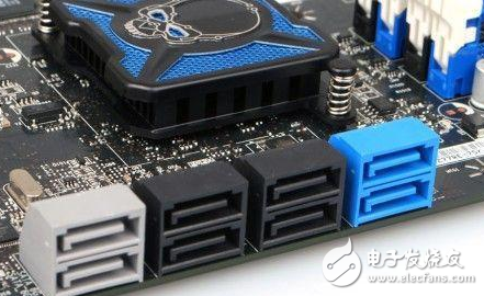
Nine, Serial ATA interface signal description1.SATA0TXP (O) Serial ATA 0 Transmit (Serial ATA0 Transfer)
2.SATA0TXN (O) Serial ATA 0 Transmit (Serial ATA0 Transfer)
This signal forms a differential signal pair with SATA0TXP for transmitting data.
3.SATA0RXP (I) Serial ATA 0 Receive (Serial ATA0 Receive)
4.SATA0RXN (I) Serial ATA 0 Receive (Serial ATA0 Receive)
This signal forms a differential signal pair with SATA0RXP for receiving data.
5.SATARBIAS (I) Serial ATA Resistor Bias (Serial ATA Resistor Bias)
6.SATARBIAS# (I) Serial ATA Resistor Bias (Serial ATA Resistor Bias)
This signal, like the SSATABIAS, is connected to a resistor connected to GND to provide a voltage offset for SATA.
7.SATALED# (OD) SATA Drive Activity Indicator
When this signal is Low, it indicates that the current SATA hard disk is reading and writing data.
Ten, IDE interface signal description1.DCS1# (O) Device Chip Select
This signal is the device selection signal For Rang 100.
2.DCS3# (O) Device Chip Select
This signal is the device selection signal For Rang 300.
3.DA[2:0] (O) Device Address
These signals are used to transmit address signals.
4.DD[15:0] (I/O) Device Data
These signals are used to transmit data signals.
5.DREQ (I) Device Request
When the IDE Device does a DMA read and write operation, it will drive this signal to send a DMnA request to the south bridge.
6.DACK# (O) Device DMA Acknowledge (Device DMA Acknowledgement)
When the IDEn Device has made a DMA request, if the current bus is idle, the South Bridge will drive a signal to delegate control to the IDE Device.
7.DIOR# (O) Disk I/O Read (Disk I/O Read)
This signal is driven by the south bridge, and when it is active, it indicates that a read operation is to be performed on the disk.
8.DIOW# (O) Disk I/O Write (Disk I/O Write)
This signal is driven by the south bridge, and when it is active, it indicates that a write operation is to be made to the disk.
9.IORDY (I) I/O Channel Ready (I/O channel ready)
This signal is driven by IDEn Device. When it is valid, it means the IDE Device is ready to be OK.
XI, LPC interface signal description1.LAD[3:0] (I/O) LPC Command, Address, Data
These four signal lines are used to transmit the commands, addresses, and data of the LPCn Bus.
2. LFRAME# (I/O) LPC Frame (LPC Frame)
When this signal is active, it indicates to start or end an LPC cycle.
3.LDRQ# (I) DMA Request
When the Device on the Super I/O needs to use the DMA Channel, it will drive this signal to make a request to the South Bridge.
Twelve, USB interface signal description1.USBP+ (I/O) USB Signal (USB signal)
2.USBP- (I/O) USB Signal (USB signal)
This signal forms a differential signal pair with USBP+ to form a USB Port for transmitting addresses, data, and commands.
3.OC# (I) Over Current
When there is a USBn Device overcurrent, this signal will pull Low, telling the South Bridge that an overcurrent has occurred.
Thirteen, SMBus interface signal description1.SMBDATA (I/O) SMBus Data (data line)
2.SMBCLK (I/O) SMBus Clock (clock line)
The above two signal lines are the system management bus, and the south bridge is used as the control center to read and write operations on some devices of the motherboard, such as multiplier IC, SPD, and the like. These two signals must be externally pulled through the resistor Pull High.
Fourteen, AC-Link interface signal description1.RST# (O) Reset (reset signal)
This signal is driven by the south bridge to initialize the Audiion Chip.
2.SYNC (O) Sync (synchronization signal)
3.BIT_CLK (I) Bit Clock (clock input)
This is a 12.288Mhz serial data clock generated by Codec to the South Bridge.
4.SDOUT (O) Serial Data Out (serial data output)
The data is sent from the South Bridge to Codec. n
5.SDIN (I) Serial Data In (serial data input)
Data is sent by Codec to Southbridge.
Fifteen, FDC interface signal description1.DRVDEN0 (OD) Drive Density Select Bit
Drive density selection signal.
2.INDEX# (I) INDEX (index)
This Pin is the Schmitt trigger input. When this is Low (active), the head is positioned by the index hole to the starting track.
3.MOA# (OD) Motor A On (Motor A is open)
When this signal is Low, motor A is started.
4.DSA# (OD) Drive Select A (drive A selection)
When this signal is Low, drive A is selected.
5.DIR# (OD) DIR (column directory)
The head stepping motor moves in the direction of When it is High, it moves outward, and when it is Low, it moves inward.
6.STEP# (OD) Step (step)
The step output pulse, when this signal is Low, will generate a pulse to move the head to another track.
7.WD# (OD) Write Data (write data)
Write data, when this signal is Low, write data to the selected drive.
8.WE# (OD) Write Enable (write enable)
Write permission, when Low means to allow writing to the disc.
9.TRACK0# (I) Track 0 (0 track)
0 track, when this signal is Low, the head will be positioned to the outermost track (0 track).
10.WP# (I) Write Protected (write protection)
Write protection, when this signal is Low, the disk slice is write-protected, and only the read data cannot be written.
11.RDATA# (I) Read Data
Read data from a floppy disk when it is Low.
12.HEAD# (OD) Head (head)
The head is selected. When it is High, the head of the 0 side is selected, and when it is Low, the head of the 1 side is selected.
13.DSKCHG# (I) Diskette Change (replace disk)
The disc is replaced. When this signal is Low, the disc can be taken out at any time during the power-on state.
Sixteen, Parallel Port interface signal description1. SLCT (I) Printer Select Status
This Pin is mainly used to select the printer mode. When it is High, it indicates that the printer is selected. There are two modes of printing that can be set to ECP and EEP.
2. PE (I) Page End (end of page)
When this signal is High, it indicates that the printer has detected the end of the page.
3. BUSY (I) Busy (printer busy)
When this signal is High, the printer is busy and not ready to receive data.
4. ACK# (I) Acknowledge (confirm)
When this signal is Low, it indicates that the printer has received data and is ready to accept more data.
5. ERR# (I) Error (Error)
When this signal is Low, it indicates that the printer has an error while printing.
6. SLIN# (O) Printer Select
This signal is checked for the printer output line.
7. INIT# (O) Initialization
When this signal is Low, it indicates that the printer is initialized.
8. AFD# (O) Auto Line Feed (automatic routing)
When the printer prints a problem with the needle, this signal will be pulled Low and the printer will automatically play it again.
9. STB# (O) Strobe (locked)
When this signal is Low, it means that the parallel data is locked into the printer.
10. PD[7:0] (I/O) Printer Data
These signals are used to transfer printer data.
Seventeen, Serial Port interface data description1.CTS# (I) Clear To Send
This signal is used for the Modem control input. This function can be tested by reading the handshake status register Bit 4.
2.DSR# (I) Data Set Ready (data preparation)
When this signal is Low, it indicates that the Modem or data placement is ready to transmit data.
3.RTS# (I/O) Request To Send
When this signal is Low, it indicates that the modem or modem is ready to send data.
4.DTR# (I/O) Data Terminal Ready (data terminal preparation)
When this signal is Low, it indicates that the data terminal is ready to communicate.
5.SIN (I) Serial Data In (serial data input)
This signal is used to receive data.
6.SOUT (O) Serial Data Out (serial data output)
This signal is used to send data.
Mobile Led Display,Led Screen Mobile,Led Screen For Mobile,Led Display In Mobile
ShenZhen Megagem Tech Co.,Ltd , https://www.megleddisplay.com