With the continuous heating of LoRa technology in the industry, coupled with its unique superior transmission performance, the group using LoRa technology is exploding, because most of the groups are in contact with the radio technology such as LoRa, the process of making products. In the middle, there are often troublesome RF circuit design problems. In fact, as long as you master a few key points, you can basically play the best performance of LoRa.
Key point 1, matching circuit designIn the schematic design, a π-type matching circuit needs to be reserved between the antenna connector and the antenna pin of the module. The impedance of the antenna is affected by factors such as the floor, casing and mounting angle of the board. This π-type matching circuit is reserved to correct the antenna to 50 ohms when the antenna deviates significantly from 50 ohms.
By default, the antenna impedance is closer to 50 ohms. C17 and C18 in the figure below do not need to be soldered; while L2 uses 220pF capacitors, or 1nH inductors, or 0 ohm resistors, all of which can be used. In the case of special situations, such as the inside of the antenna mounting mold, the small size of the antenna or the need to strengthen the harmonic suppression, these three matching components need to be matched and adjusted.
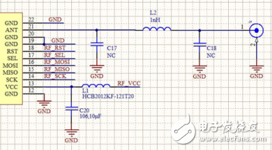
[Figure 1] Reserved matching circuit for LoRa module application
In theory, regardless of the antenna impedance at any value, it can be matched to 50 ohms by a π-type matching circuit. However, in fact, the inductance and capacitance have internal resistance. This internal resistance will absorb energy. If the antenna impedance is too small (a few ohms) or large (thousands of ohms), it will lose its meaning by matching it to 50 ohms through the matching circuit. . The reason is that most of the energy has been consumed on the internal resistance of the matching component.
Point 2: Microstrip line routing rulesThe microstrip line referred to herein refers to the PCB trace between the antenna pin of the LoRa module and the antenna connector. The following figure shows an example of the microstrip line on the LoM module ZM470SX-M evaluation board. Since the internal impedance of the module and the antenna impedance are all designed with a 50 ohm standard, when the microstrip line characteristic impedance is also 50 ohms, the three get the most. Good match.
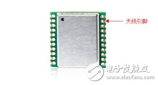
[Figure 2] LoRa module stamp hole antenna interface
In order to obtain a microstrip line of about 50 ohms, on the one hand, it is possible to provide impedance processing requirements to the PCB manufacturer. A capable PCB manufacturer can control the trace impedance according to the line width of the board parameter; on the other hand, the board can be obtained from the PCB manufacturer. After the parameter (main is the dielectric constant), the line width is calculated by the software itself to control the impedance to the range we expect.
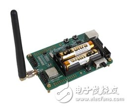
[Figure 3] LoRa Learning Evaluation Board
According to experience, if the FR4 plate is used (the dielectric constant is between 4.2 and 4.6), the characteristic impedance is closer to 50 ohms when the line width is 2.2 times the distance from the microstrip line to the reference layer. For example, in the case of a double panel, when the thickness is 0.8 mm, the line width can be 1.7 mm. However, it must be noted that the paving below the microstrip line must be complete, and the microstrip line and copper spacing are set according to the calculation results of the impedance calculation software. The ground pads on both sides of the module antenna pins must be well grounded.
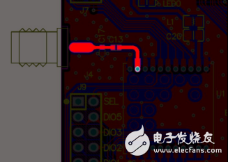
[Figure 4] ZM470SX-M evaluation board microstrip line example
Since the wavelength of the 470MHz electromagnetic wave is long, if the length of the microstrip line does not exceed 20mm, the characteristic impedance of the trace has a little effect on the performance in the range of 25~75 ohms. In this case, it is recommended to use a line width of 25mil.
Point three, PCB floor requirementsWe have encountered a lot of situations where users use our modules on the product, use the same configuration parameters as our evaluation board on the product program, and use the antenna on our evaluation board, the communication effect is significantly better than our evaluation board. A lot worse. The communication distance is nothing more than the three key parameters of transmission power, receiving sensitivity and antenna. The first two parameters are tested when our module is out of the factory. The unqualified products are disposed of when the waste is processed, and the antenna is It varies depending on the user's design. The distance that affects communication is mainly the parameter of the antenna. The other two parameters are hardly changed greatly due to the difference of the user's board.
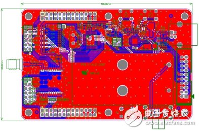
[Figure 5] ZM470SX-M evaluation board PCB example
In air, the electromagnetic wave with a frequency of 470MHz has a wavelength of 63CM. If a standard half-wave dipole antenna is designed, the antenna has at least half a wavelength, which is 31.5CM. In practical applications, most of the products do not reserve such a large space for the antenna design, so the spring antenna is generally used. When using this kind of spring antenna, the antenna is connected to different boards, and the performance parameters are different. This is because this type of antenna, the spring is only a part of the whole antenna, and the other part is the ground on the circuit board, so it must be paid attention to when the circuit is laid. The general principle is: First, the antenna should be vertical The circuit board is installed, and the second is to make the copper block of the paving floor as large and continuous as possible, and relying on dense via holes to make the paving of the front and back sides continuous is also feasible.
Point 4, antenna installation specificationsAfter all the hardware parameters are adjusted, the installation of the antenna is also a key step. The antenna radiation is directional. It is not the energy radiated in each direction. As we speak, the sound heard in some directions is strong, and some directions are heard. weak. When installing the antenna, it is necessary to align the antenna with the strongest radiation direction to the receiving antenna. The receiving antenna is likely to obtain the strongest received signal. To do this, the radiation direction of the antenna must be known.
In the absence of a professional antenna test laboratory such as a darkroom, how do you test the radiation direction of the antenna? After finalizing the product, we can continuously send the data, and use the spectrum analyzer to test the signal strength at a certain distance from the product, rotate the tested product, and record the signal strength in all directions, so that the antenna radiation of the product can be drawn. General direction map.
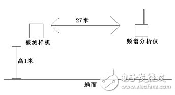
[Figure 6] Radiation direction test
When installing near reflective surfaces such as walls, doors, and metal surfaces, attention must be paid to the effects of reflections. The theoretical and test results prove the following conclusions:
Best location:  Worst position:
The best and the worst position are alternately spaced λ/4;
RX1 is better than RX2. For example, at 470MHz, the effect of 16CM from the reflective surface is much better than 32CM.
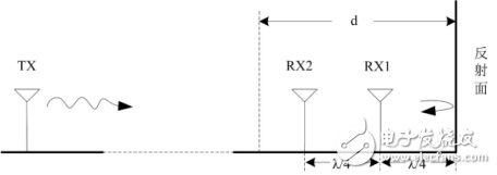
[Fig. 7] Reflection of electromagnetic waves
Portable Speaker,Speaker Receiver,Outdoor Speakers,Wireless Speakers
GUANGZHOU LIWEI ELECTRONICS CO.,LTD , https://www.gdliwei.com