Overview
In recent years, mobile devices such as notebook computers have achieved up to 100W charging, and more and more USB PDs have been used to make charging connectors universal. In addition, the trend of using both wired charging and wireless charging (wireless power supply) at the same time has also increased. However, to meet the wide range of power requirements such as USB PD, for example, to charge 2 batteries (=8.4V) from a 5V charger, the system must add a boost function. In addition, adopting two kinds of charging methods at the same time, need to increase charging IC and external component again, and control and charge the switch through the microcontroller, these in the engineering practice, the complexity and cost will bring no small pressure.
In response to these problems, ROHM has launched a new battery charging IC: BD99954GW/MWV. This chip uses 1-4 cells as the object, uses the buck-boost control to generate a charge voltage of 3.07-19.2V, and supports the battery charging IC of the most advanced USB PD system. Realize ROHM's original, industry-first charging system dual input function, and equipped with charging adapter judgment function, can carry out charge switching without microcontroller control. In addition, it not only supports the USB PD standard, but also supports the most popular USB BC1.2 charging standard today. USB charging, wireless power supply, AC adapter charging and other charging methods can be easily implemented, which is very helpful for creating a more convenient charging environment.
With the increasing popularity of wireless charging technology, most modern chargers need to be compatible with both wired and wireless input sources. Such a circuit is built using BD99954, which can eliminate the switching circuit in the traditional design method:
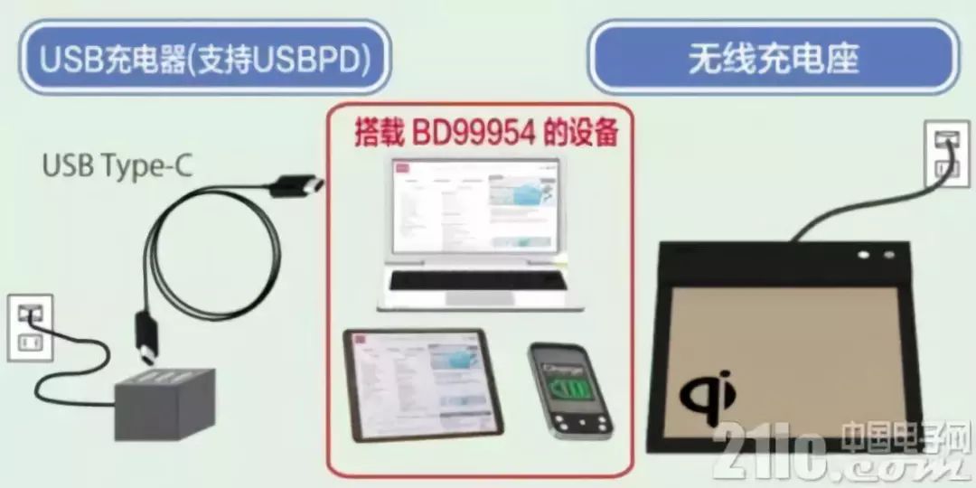
Figure Using BD99954 to Design Dual Input Power Supply
BD99954GW and BD99954MWV have the following two features, which are very helpful for creating a more convenient charging environment:
(1) The industry's first support for dual system charging. Dual input mode makes it easier to import the two charging methods. In addition, a charging adapter determination function is also provided so that the charging can be switched without a microcontroller. The two-input charging system does not need to be equipped and adjusted (charging path switching, preventing current backflow). The external components, transistors, and resistors required for separate processing not only have a smaller mounting area, but also contribute to greatly reduce the design burden.
(2) Boost pressure control to support the most advanced USB PD system. With the buck-boost control, any voltage from 5-20V (the maximum voltage of the USB PD) can generate the charging voltage required for battery charging. For example, when charging with two cells (=8.4V), 8.4V can be stepped down at 20V input, 8.4V can be charged after 5V input.
In addition, the USB charging standard not only supports the USB PD, but also supports the most popular USB BC1.2. Therefore, it supports multiple charging methods from conventional USB charging to USB PD charging. This article uses the evaluation board that ROHM developed for this chip: The BD99954MWV Evaluation Kit makes an evaluation of the function of this chip, and explores some features of its use method and function.
First look at the BD99954 development board:
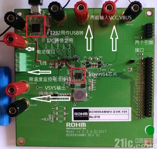
Figure development board and its main components
Note that the BD99954 development board is an engineering sample. Therefore, there is a flying line and it does not affect the functional evaluation of the chip.
hardware
Schematic
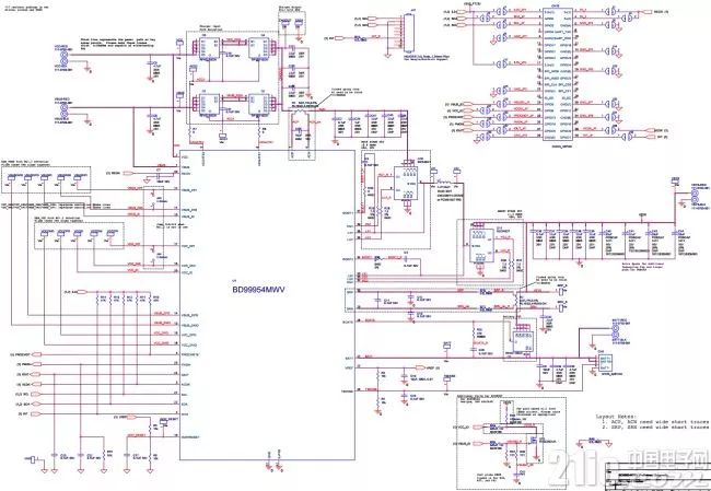
Figure Schematic 1 (Main Circuit)
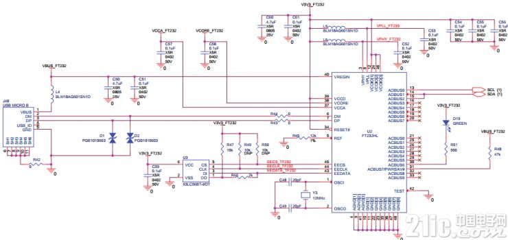
Figure Schematic 2 (USB to I2C section)
Due to the problem of resolution, the schematic diagram is not clearly displayed on the page. Interested students can look for the pdf file in the reference resource at the end of the text.
The whole schematic is relatively simple and there is nothing to say. The main components are two chips (BD99954+FT232HL) and some passive components. Which FT232HL is used to communicate with the software on the PC, so the entire development board is mainly BD99954 and passive devices. It can also be seen that BD99954 is highly integrated.
chip
Below from the chip to analyze this chip, look at the typical application diagram:
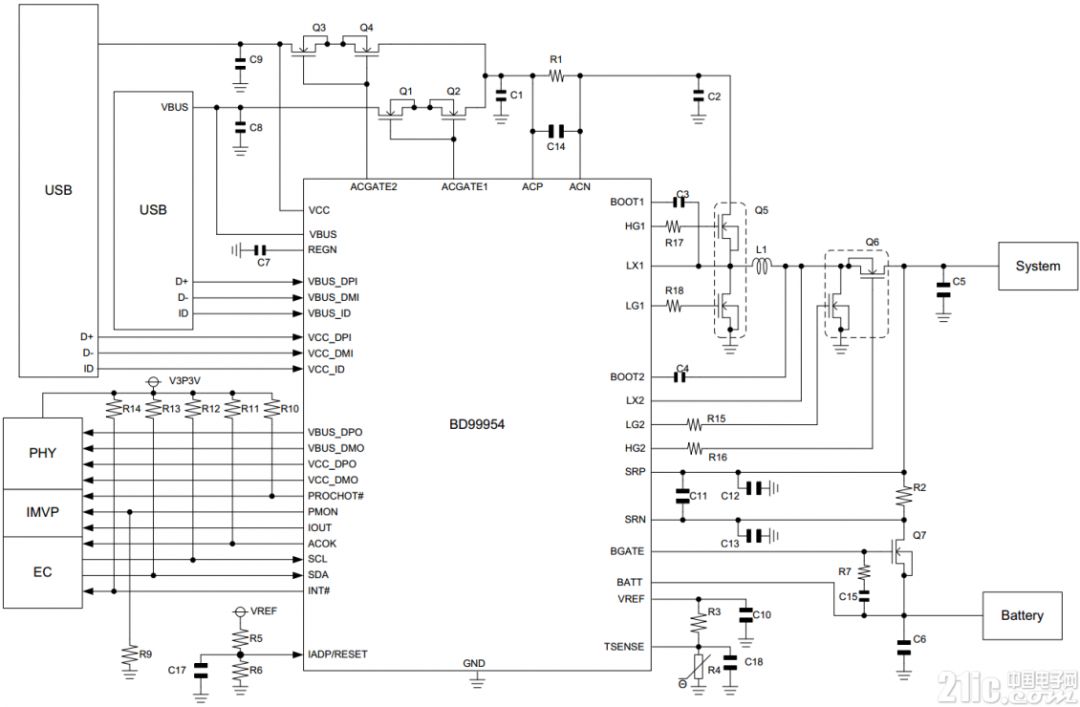
Figure BD99954 Typical Application
Look at the internal block diagram of the chip:
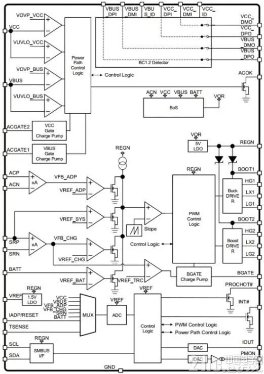
Figure BD99954 internal block diagram
From the above two figures, it can be seen that the chip integrates some common units in the power management circuit, which greatly simplifies the final circuit.
Dual input automatic switching
For example, if two input sources are to be switched, the previous design:
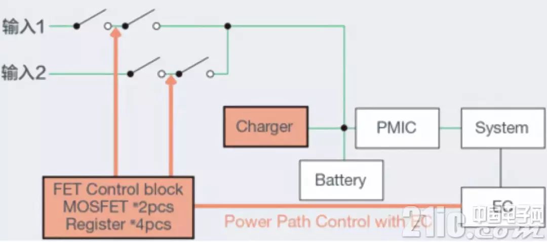
The previous two-input switch requires additional switching circuits
If the same function is designed using the BD99954, it can be greatly simplified. The switching FET and the power bank in the above figure can be omitted:
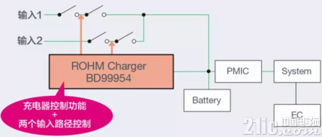
Figure Using Dual Input Switching with BD99954 Design
Charging curve
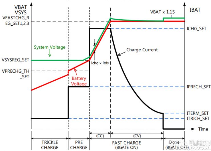
Chart charging curve
System Voltage is the operating voltage of the system. If the battery voltage is lower than this voltage, the battery must first be charged to this voltage using the trickle and precharge modes. After that, increase the charge current into the fast charge constant current mode and charge the battery to the preset full charge voltage. At this point, the battery is not fully charged. At this time, it enters the fast-charged constant-voltage mode until the battery voltage is 1.15 times the set VBAT. The battery can be considered fully charged at this time. All of the above parameters can be set via the I2C bus. In addition, in order to prevent the battery from overheating, the chip can also monitor the temperature of the battery through the temperature detection end of the battery. When the temperature is too high, the current is halved, and the voltage is output according to the voltage set in the third gear according to the temperature.
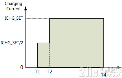
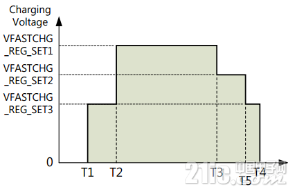
Figure constant current and constant pressure parameters decrease according to temperature monitoring
GUI configuration software
Manufacturers have specially developed GUI software for this development board to facilitate the rapid evaluation of their functions. The download address is at the end of the document. How to install not to say, the software is divided into three interfaces:
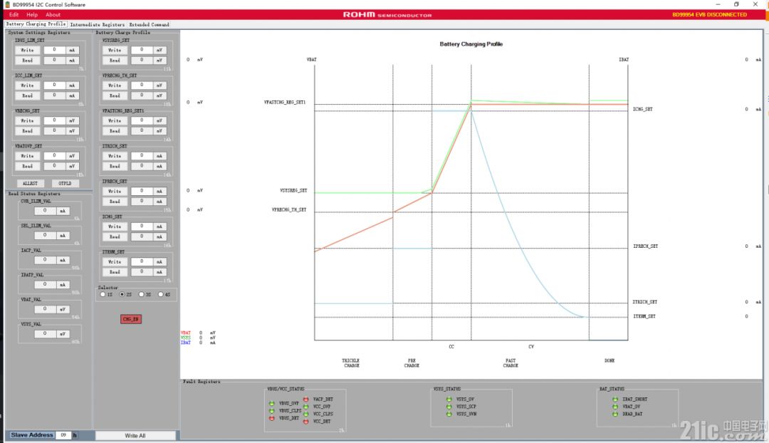
Charge and discharge control interface
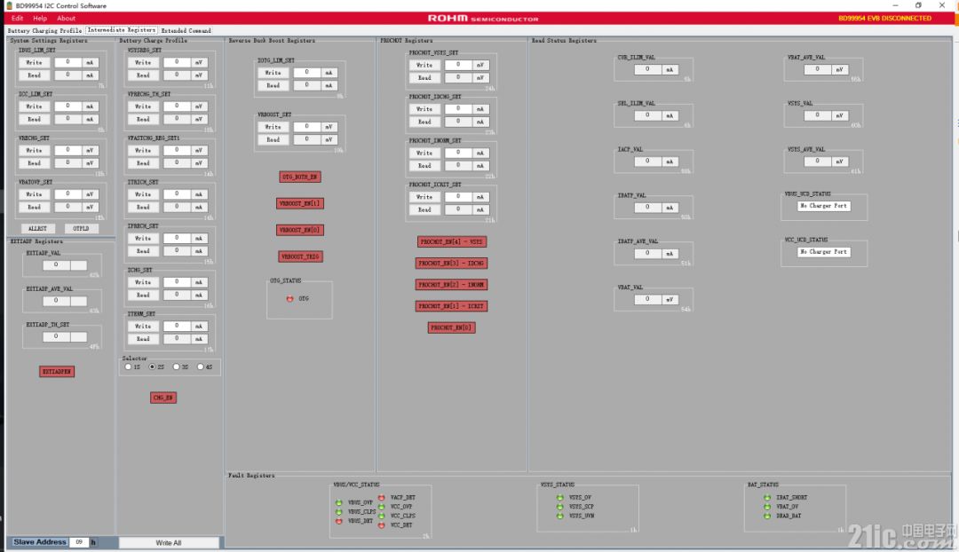
Figure direct control register interface
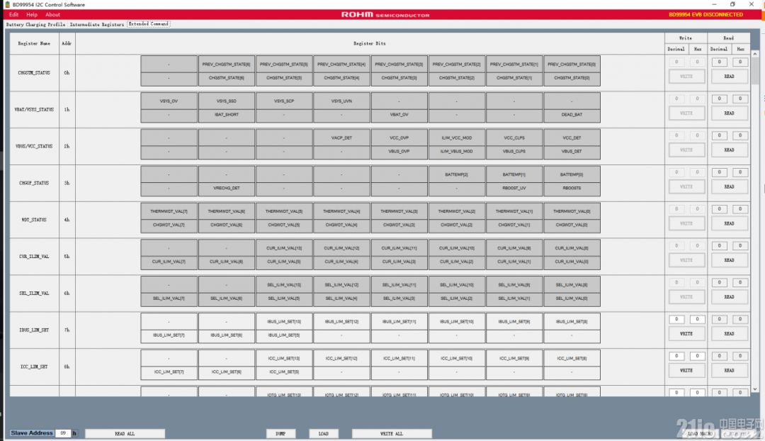
Figure expansion control interface
Function demonstration 1: Two-way power supply automatically switches charge and discharge
Charging connection:
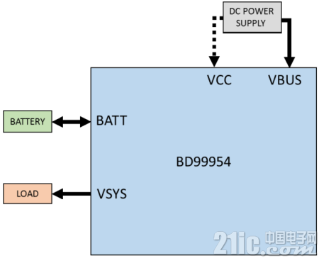
Figure charging connection
The discharge connection is similar to the above except that the battery is not connected and the voltage is output from VSYS.
First of all, to observe the dual power switch, disconnect the 5V input of VCC, do not connect the battery, only connect 20.5V laptop power supply (modified) on VBUS, configure it to output 19.2V, the software configuration is as follows:
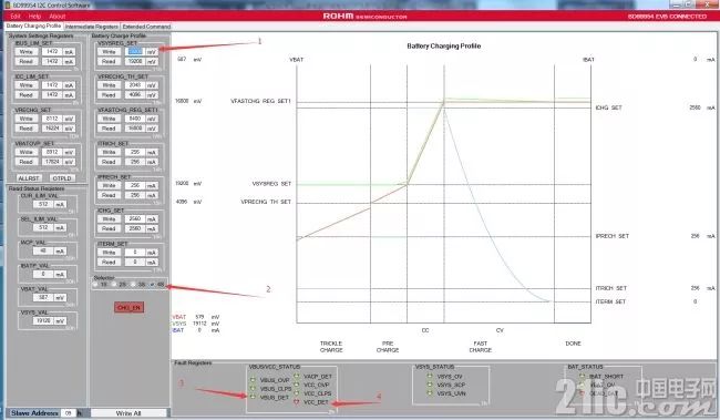
Figure Experiment 1 Configuration UI
Pay attention to several points: First adjust the mode to 4S, that is, 4 series mode, otherwise the chip will not allow such a high voltage output. Second, the output voltage can theoretically be configured to 32,752 mV, but the chip can only output 19,200 mV, so the configuration will be automatically set by the software upper limit. The last 3, 4 points are the VBUS, VCC monitoring indicators, and the green light indicates that the input is detected. The figure shows only VBUS input.
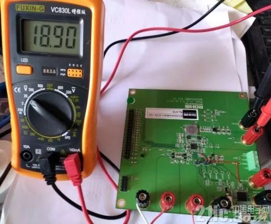
Figure experiment 1 result
Note here that my accuracy of this multimeter is not good.
Now that 5V VCC is also connected, VBUS is used by default when both inputs are simultaneously connected. This can also be used to change which input is used in favor of the register.
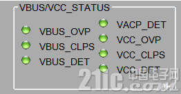
Figure two input simultaneous access
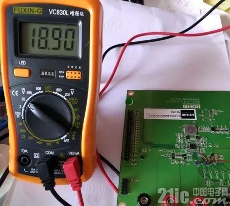
At this point, the output is still 19200mV, which is expected
Turn off VBUS and only access VCC:
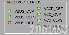
Diagram only access VCC (5V)
At this time still output 19200mV, pay attention to this time for the boost mode.
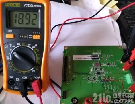
Figure VCC (5V) Boost to 19200mV Output
Let's take a look at the charging mode. The chip can charge 1-4 series lithium-ion batteries in series. The authors did experiments separately. However, due to the more troublesome pictures, only single-cell batteries are shown here.
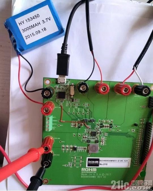
Figure access battery
Note that if the battery has a temperature resistance, you can access the green military carrier in the picture above. Temperature resistors have been used to prevent overheating. However, the author does not have such a battery on hand and for the time being does not experiment with this function.
For charging, you need to configure the following parameters:

Charging parameters
1. Charging voltage: The battery less than this voltage is either protected or overcharged, requiring trickle charge before this voltage
2. Precharge voltage: less than this voltage requires pre-charge
3. Precharge current
4. Fast charge current
5. Fast charge voltage: This voltage can be reached to enter the normal charge mode
6. Turbulence current
7. End current, some batteries require a certain termination current to prevent leakage
8. After the configuration is completed, press this button. When it turns green, it starts charging. At the same time, the right interface starts to display the actual charging curve.
The above content can be matched with the above charging curve section.
Feature Demo 2: Battery Reverse Power
Reverse power connection:
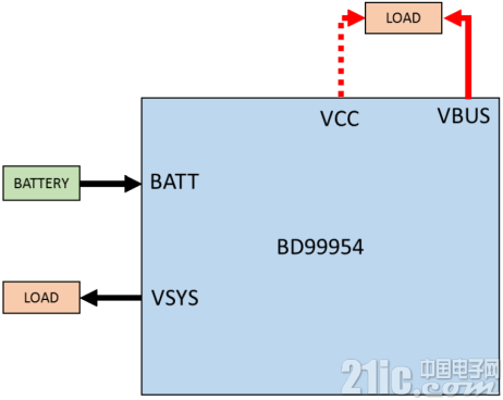
Figure battery power supply
When both external power supplies are turned off, the batteries need to be reversed. Turn off the two inputs first. Note that the battery must be connected and higher than 3.8V at this time. Otherwise, the entire board will not have power or control.
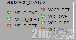
Figure two output are broken
When the power is reversed, it is necessary to confirm that both inputs are turned off. Otherwise, the short circuit will burn the device.
The configuration of reverse power supply is on the second interface. By default, it is off. Both VCC and VBUS interfaces can configure the output.
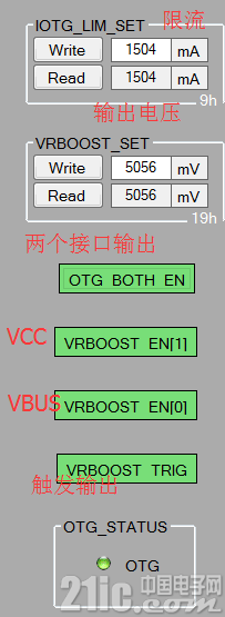
Figure reverse output configuration
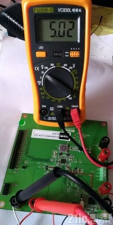
Figure reverse buck boost output
Feature Demo 3: Custom Control
According to the schematic diagram posted above, the official configuration software controls the BD99954 chip through the USB to I2C interface. In this case, if custom control is to be performed, the user can additionally use the master chip to perform the I2C bus. Of course, most applications do not need this kind of custom communication because the chip itself has common detection and switching functions. This article only shows one possibility for users with advanced custom control requirements.
In addition, the GUI software provided by the official company has the function of script programming for custom control. However, it may be the reason for the engineering test version. It has not been successfully run on my computer. However, this is not a big problem, either because the actual application either does not control the work of the default configuration, or it will be controlled by the external master through I2C.
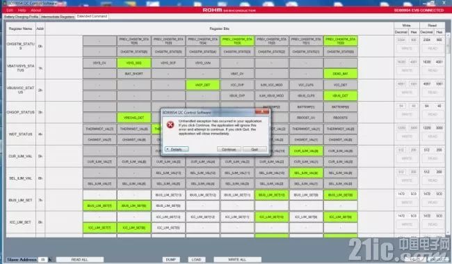
Figure MCR Runs Abnormally
The I2C device address of BD99954 is 0x09, and the rate is 10KHz to 400KHz. Its read/write format and waveform are as follows:

Figure read word format

Figure write word format
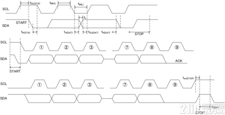
Graph communication waveform
This shows that its communication is no different from the general I2C device, as long as the I2C bus can communicate with it according to its command format. There are three sets of command sets for the chip: basic/extension/debugging, which is switched by the MAP_SET command:
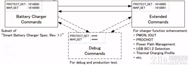
Figure command set switching diagram
Please refer to the data sheet for specific orders. Not listed here.
This uses the Arduino Uno development board to communicate with it. Connection signal on J47:
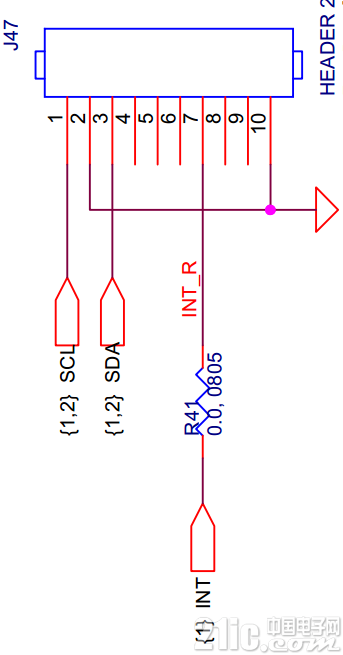
SCL/SDA signal on Figure J47
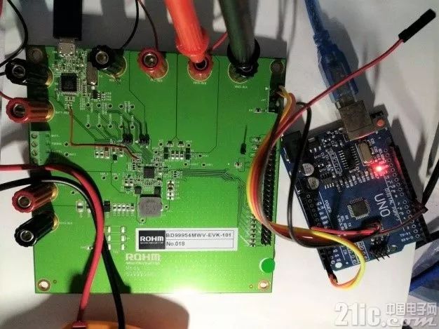
Picture BD99954+Arduino Uno
Here to configure the reverse output to 7V as an example, the code is as follows:
//Arduino Uno control the BD99954 chip.
//Author:
#include
#define BD_ADDR 0x09
//Bit 14 Trigger VRBOOST
#define VIN_CTRL_SET 0x0A
#define VRBOOST_SET 0x19
#define CHIP_ID 0x38
#define CHIP_REV 0x39
#define MAP_SET 0x3F
Void setup() {
Wire.begin(); // join i2c bus (address optional for master)
pinMode(LED_BUILTIN, OUTPUT);
pinMode(7, INPUT);
Serial.begin(115200);
}
Void wr16(uint8_t cmd, uint16_t d16)
{
Uint8_t dl = (uint8_t)d16;
Uint8_t dh = (uint8_t)(d16>>8);
Wire.beginTransmission(BD_ADDR); // transmit to device
Wire.write(cmd);
Wire.write(dl);
Wire.write(dh);
Wire.endTransmission(); // stop transmitting]
}
Uint16_t rd16(uint8_t cmd)
{
Uint16_t ret16 = 0;
Wire.beginTransmission(BD_ADDR); // transmit to device
Wire.write(cmd);
Wire.endTransmission(); // stop transmitting]
Wire.requestFrom(BD_ADDR, 2);
While (2 != Wire.available())
{
digitalWrite(LED_BUILTIN, !digitalRead(LED_BUILTIN));
}
Uint8_t dl = Wire.read();
Uint8_t dh = Wire.read();
Ret16 = ((uint16_t)dh << 8) + dl;
Return ret16;
}
Void loop() {
Uint16_t map_set = rd16(MAP_SET);
Serial.println("MAP_SET:");
Serial.println(map_set, HEX);
Uint16_t tmp = rd16(CHIP_ID);
Serial.println("CHIP_ID:");
Serial.println(tmp, HEX);
Tmp = rd16(CHIP_REV);
Serial.println("CHIP_REV:");
Serial.println(tmp, HEX);
Tmp = rd16(VRBOOST_SET);
Serial.println("VRBOOST_SET:");
Serial.println(tmp, HEX);
Wr16(VRBOOST_SET, 7000);
Tmp = rd16(VRBOOST_SET);
Serial.println("VRBOOST_SET:");
Serial.println(tmp, HEX);
Tmp = rd16(VIN_CTRL_SET);
Serial.println("VIN_CTRL_SET:");
Serial.println(tmp, HEX);
Delay(50000);
}
Output:
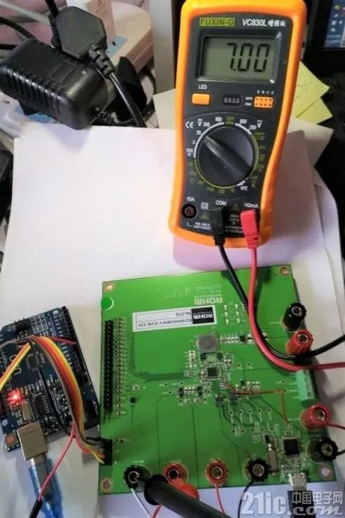
Diagram Control Board Output via I2C
Conclusion
BD99954 has a high degree of integration, and it covers almost all the functions of power management in applications such as notebooks/tablets/smartphones, which greatly reduces the design burden on engineers and improves product stability.
Guangzhou Yunge Tianhong Electronic Technology Co., Ltd , https://www.e-cigarettesfactory.com