Noise and interference on analog audio channels in cellular phones are usually due to demodulation or common / bad grounding from the radio frequency to the audio band.
When a high-energy radio frequency signal from a telephone antenna is received, an audio circuit with a relatively low bandwidth in the phone will erroneously demodulate the radio frequency transmission signal. This will worsen the noise background of the audio channel. A certain technique and structure can be adopted in the audio amplifier circuit to minimize this deterioration effect, and placing a suppression component next to the input pin is an inexpensive remedy. Low-value ground capacitors are often used because designers usually choose the lowest capacitor impedance according to the RF carrier frequency.
Integrating all the commonly used analog audio input / output functions into a single IC is a very effective solution, which can minimize the impact of common / bad grounding. This is actually transferring the most troublesome and troublesome grounding problem from the printed circuit board layout engineer to the IC manufacturer. In addition to including the necessary analog audio input / output functions, this IC must also provide a digital audio interface sufficient to support the voice band and any multimedia functions (such as application processors). The IC should also provide partition shutdown control for different cells to maximize battery life.
The following focuses on some analog / digital audio issues that arise in a single-chip solution. We start with MAX9851, a technical solution that simplifies the design of GSM / GPRS cellular phones as a model.
Analog audio—High-gain audio circuits that reduce microphone noise, such as microphone amplifiers (microphone amplifiers), are most affected by poor grounding. This is especially true for single-ended circuit structures. In this type of circuit, the small voltage difference between the reference ground of the microphone amplifier and the reference ground of the signal source (in this case, the GND pin of the microphone) is amplified into the signal path. In complex products like cellular phones, the ground plane of the audio part is often shared with other circuits. Since the copper ground plane is not "zero ohm" (we often think so), this will cause performance degradation. Therefore, if any current flows through this limited resistance, a small potential difference will be generated on the ground plane.
The grounding problem can be solved with a fully differential input microphone amplifier. This method has been adopted by the MAX9851. In fact, it uses the differential input to remotely sense the microphone's GND pin. After remote sensing is used, the AC voltage difference between the CODEC reference terminal and the microphone GND appears as a common mode signal to the microphone amplifier. This voltage difference is attenuated by the common-mode rejection ratio of the amplifier, thus significantly reducing its equivalent noise contribution to the signal path. The only cost of this design is the need for an additional printed circuit line between the microphone and the CODEC, and the addition of a coupling capacitor.
The MAX9851 can also be switched to an external stereo microphone input to replace the internal microphone. This input usually comes from the car hands-free or other external headphones. In this case, the EXTMICGND pin "Kelvin senses" the two channels L and R, and the input CMRR of the amplifier can be used to eliminate ground noise. The wiring of the printed board of EXTMICGND should extend all the way to the GND end of the car's hands-free socket or headphone jack for best results (Figure 1).
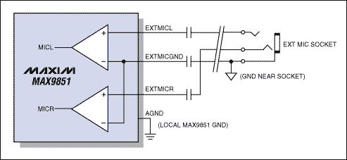
Figure 1. Using a differential amplifier to reference the "ground" of a remote sensing socket. Any AC voltage between the internal ground and the socket ground is greatly suppressed and not amplified by the microphone amplifier gain.
The microphone bias circuit also introduces significant noise into the signal path. Most of the bias voltage noise will appear directly at the input of the microphone amplifier. A more reasonable microphone amplifier design, as integrated in the MAX9851, should provide a low-noise bias voltage that is adjusted to match the output noise level of the microphone amplifier input noise level.
Analog audio—stereo DirectDrive ™ headphones and receiver outputs require high-quality headphone audio playback circuits to play compressed music files with sound quality close to CD. The signal-to-noise ratio (SNR), linearity, and bandwidth are greatly improved over the basic 300Hz to 4kHz voice channel. Low frequency expansion may be problematic because the headphone driver usually requires a series capacitor to prevent the DC bias of the headphone amplifier from entering the headphone. The typical impedance of common stereo headphones can be as low as 16Ω, and it and the series capacitor form a high-pass filter, which has an attenuation effect on low-frequency components. To extend the low frequency response, for example down to 100Hz, two 100µF DC blocking capacitors are needed for 16Ω stereo headphones.
Using Maxim's DirectDrive technology can remove these two series capacitors, because the output of the amplifier is referenced to 0V. The low-frequency component in this case is limited by the DC filter (digital source, as designed in the MAX9851), or by the input coupling capacitance on the input of analog sources such as lines or microphones. Another advantage of the DirectDrive design is that when it leaves or enters the shutdown mode, the cause of clicks / pops is fundamentally eliminated. Because there is no series capacitor, there is no need to charge or discharge the capacitor, and no net current flows through the headphones during the on / off process.
The stereo headphone output of the MAX9851 can also work in bridge mono mode (Figure 2) in order to be compatible with different headphones and accessories. The same socket can be used for either stereo headphones or mono headphone (microphone switch and speaker). In this mode, the output is still referenced to ground, and there is no DC voltage on the headphone cable. Therefore, the chance of short-circuit failure is much smaller.
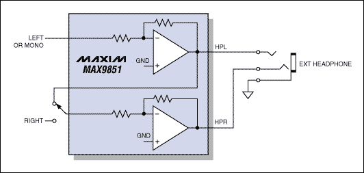
Figure 2. DirectDrive headphone output can work in bridge mono or stereo mode. Maxim's proprietary ground-referenced output means that series coupling capacitors are no longer needed, saving cost and PCB space.
The receiver output is also powered by the charge pump in the Direct Drive design, so that the output is still single-ended, allowing the negative terminal of the speaker to be connected to GND (0V). The output still has almost the same voltage swing as the more typical BTL (differential) output because the inverting charge pump provides a negative supply rail with an absolute value almost equal to the applied AVDD. The peak-to-peak output of the final output to both ends of the receiver speaker can almost reach 2 x AVDD.
Analog Audio—The Class D speaker amplifier MAX9851 integrates Maxim ’s third-generation Class D technology to drive 8Ω (or 4Ω) speakers. The advantage of Class D (switching) amplifiers over Class AB (linear) amplifiers is mainly in efficiency. Class AB amplifiers dissipate a lot of power in the output components unless the amplifier is driven to the clipping state. However, since the output element of the class D amplifier works in the switching state, its heat consumption is much smaller, so it can extend the battery life. If the cellular phone is frequently used in speaker mode, or supports push-to-talk (PTT) mode of operation, the extended battery life will be very significant.
However, special care needs to be taken when using Class D structures, especially when used in products whose core function is radio frequency transmission / reception, such as cellular phones. The rapid switching edges generated during the operation of high-efficiency class D amplifiers can cause radio frequency radiation problems, especially when PCB wiring and speaker leads are long. In order to deal with the problem of radio frequency radiation, the stereo Class D speaker amplifier in the MAX9851 uses the company's proprietary EMI suppression technology (actively limits radiation). At the cost of slight efficiency reduction, the radio frequency radiation on the speaker leads / wiring is greatly suppressed. Superb IC construction technology minimizes the interference of the D-type switching output stage to other sensitive low-noise analog circuits in the CODEC.
The stereo amplifier can work directly on a single-cell lithium-ion battery without voltage adjustment, and can output 1W of power to an 8Ω speaker when working on a 4.2V power supply (Figure 3). If you use a lower impedance speaker, you can also output higher power, but it is difficult to find 4Ω in the small-diameter speakers commonly used in cellular phones.
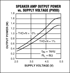
Figure 3. The stereo Class D speaker amplifier in the MAX9851 can work directly on the battery voltage, and can provide 1W continuous output (at 10% THD + N, 1kHz signal) under a 4.2V power supply.
Digital audio—a common architecture, and signal flow to realize a call—a basic function of GSM / GPRS cellular phones, requires the system to provide an ADC / DAC channel with a sampling rate of 8 kHz (or 16 kHz), with 16-bit depth in both directions. In the MAX9851, this input / output channel is fully synchronized to the 13MHz (or 26MHz, corresponding to fS = 16kHz) MCLK input to ensure that there are no lost or repeated samples. The S1 digital input / output interface can work in the GSM voice mode (Figure 4) and can provide an interface for this basic function. S1 digital interface can work in master or slave mode.

View larger image Figure 4. The S1 output in GSM voice mode supports basic GSM voice conversion functions. It can work in master or slave mode, slave mode requires the host to provide BCLK and LRCLK clock.
Many mid-range and high-end phones also generally require DAC functions with higher digits and sampling rates. For example, use it to play WMA / MP3 music or generate ringtones for WAV files. Integrating the digital-to-analog conversion used for this function with the converter used for voice is helpful to improve the integration and make all data conversion tasks centralized in one "point source". Such integration is very useful in product design. If you try to synthesize two functions in the analog domain, you will inevitably encounter problems such as ground loops and audio level differences.
Therefore, using a converter to integrate voice and multimedia data seems to be an ideal solution. The main difficulty of this method is that all voice conversion must remain synchronized to the GSM / GPRS rate (controlled by the MCLK input). For multimedia playback, an irrelevant sampling rate is usually required: for example, 44.1kHz or 48kHz. The MAX9851 uses an algorithm similar to sample rate conversion (SRC) to process digital input data. This solves this problem, so a single DAC can be used to convert voice and multimedia combined data in a synchronized manner.
In slave mode, the sampling rate of input GSM voice data must be kept accurate (controlled by MCLK). The internal digital PLL is locked to the LRCLK input of the S2 digital interface in order to accurately (average of multiple samples) playback of asynchronous multimedia audio data. In the main mode, the voice data is still accurately aligned to the required MCLK integer frequency division, but the S2 LRCLK data rate is only an approximation, with a slight fS error, and usually will not have a significant impact. Both S1 and S2 inputs can support sampling rates from 8kHz to 48kHz.
The MAX9851's S2 digital input / output interface supports I²S and other popular small variants. When not working in GSM voice mode, the S1 interface can also be programmed to support I²S, providing maximum interface flexibility to meet the needs of multi-function high-end phones.
Digital audio—GSM filter As shown in Figure 5, there is an additional filter on the S1 digital input / output interface, which can be enabled in GSM voice mode. These digital units are a highly efficient implementation of strictly regulated low-pass and high-pass filters. They suppress energy near the Nyquist frequency and low frequency bands. The filter has been proven to help meet noise and signal leakage specifications, making it easier for phones to pass tests and certifications. Figure 6 shows the frequency response of the filter.
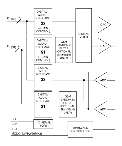
Figure 5. The MAX9851 integrates two sets of independent digital audio input / output interfaces (S1 and S2). For DAC playback, each interface can run at a different, non-integer-related sampling rate, which can be used in either master mode or slave mode.
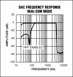
Figure 6. Frequency response of the GSM playback channel after enabling the GSM filter. At fS = 8kHz, notice the steep roll-off just before the Nyquist frequency (4kHz). You can also choose to disable high-pass filter (HPF) operation.
Conclusion The above example only highlights the few issues that a cellular phone system designer / architect must solve. The design cycle of this terminal application is getting shorter and shorter, and the integration of performance is constantly improving and changing, almost every model is different. Therefore, it should make sense to invest a certain amount of time to select a core chipset with good engineering planning, flexible application, and comprehensive functions.
Low-noise analog circuits interface with multiple playback / recording systems at different sampling rates, and control of this part of the circuit is only part of the overall design task. It is also important to integrate the following features in one solution: Analog functions and high-performance single-point digital / analog audio interfaces Flexible digital interfaces Comprehensive power management and partition shutdown These features involve a lot of system design, architecture and layout issues. The MAX9851 is a 48-pin, 7mm x 7mm single-chip solution that can be used to solve these problems, providing a solid foundation for audio design in mid- to high-end GSM / GPRS cellular phones.
Slim Led Panel Light includes round and square two shape frame. This type of thin light body is ultra slim and easy to install. It is made by aluminum frame and iron back cover. We are the manufacturer of producing energy saving interior lighting. There are three color temperatures with cool white, warm white and natural white of panel lights. Besides it is adjustable among the three color temperatures. The unique feature of led Slim Panel Light is: CRI>80, PF>0.5. These panels are mainly apply to home, office and school, etc.
Slim LED Panel Light
Led Slim Panel,Slim Panel Light,Ultraslim Led Panel,Led Panel Ultraslim
Jiangmen Lika Lighting Electrical Appliances Co., Ltd , https://www.lika-led.com