For analog CMOS (Complementary Symmetric Metal Oxide Semiconductor), the two main hazards are static and overvoltage (signal voltage exceeds supply voltage). Knowing these two major hazards, users can respond effectively.
Static electricityThe hazard caused by the electrostatic voltage formed by static charge accumulation (V = q / C = 1 kV / nC / pF) may break through a thin layer of oxide (or nitride) that insulates between the gate and the substrate. This hazard is small in normal operating circuits because the gate is protected by an on-chip Zener diode that can cause charge loss to a safe level.
However, when plugged into a socket, there may be a large amount of static charge between the CMOS device and the socket. If the first pin of the plug-in socket happens to be without a Zener diode protection circuit, the charge on the gate will be released through the oxide layer and damage the device.
The following four steps help prevent the device from being damaged during the system assembly phase:
Store unused CMOS devices in a black conductive foam material to prevent charge buildup between pins during transport;
The operator responsible for the device plug should be connected by a plastic strip is connected to the system power ground;
Before removing the CMOS device from the protective foam material, the foam material should be co-located with the power source to release the accumulated charge;
After the circuit is inserted into the board, the board should be grounded or shielded when moving the board .
SCR latchWhen using analog CMOS circuits, it is safest to ensure that no analog or digital voltages that exceed the supply voltage are applied to the device and that the supply voltage is within the rated range. Nevertheless, it is necessary to carry out overvoltage protection. If you understand the mechanism of the problem, the protection measures will work well in most cases.
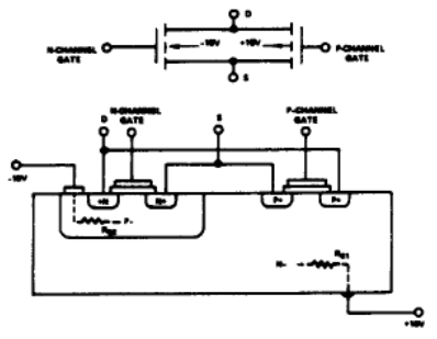
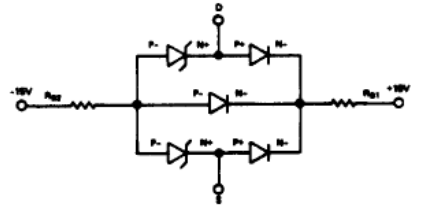
Figure 1 is a circuit diagram and a cross-sectional view of a typical CMOS output switching unit. From the connection between different units and regions, we can draw an equivalent diode circuit diagram (Figure 2). If the analog input voltage at the S or D terminal exceeds the supply voltage.

Figure 1: Circuit diagram and cross-sectional view of a typical CMOS output switching unit

Figure 2: Equivalent Diode Circuit Diagram
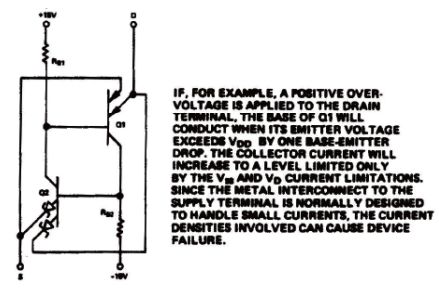
Produced by different parasitic transistor will be forward biased diode junctions mode. These parasitic NPN and PNP transistors form an SCR (Silicon Controlled Rectifier) ​​circuit as shown in FIG.

Figure 3. Parasitic transistor in a CMOS switch
Overvoltage can cause excessive current and metallization problems. Typically, the output of the operational amplifier or as a voltage source terminal S of the D terminal, the operational amplifier so that the current is not greater than the DC output current limit. However, transient induced currents can still damage CMOS devices; therefore, protection is necessary.
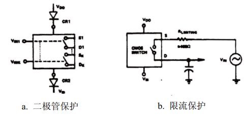
Figure 4 illustrates a method to prevent parasitic transistors from turning on by a series diode (such as 1N459) on the power supply pin . If the S or D terminal voltage is higher than the supply voltage, CR1 and / or CR2 are reverse biased, and the base drive circuit cannot turn the transistor on. Each CMOS device should have a separate pair of diodes to protect it. Although this method is effective, it is not foolproof. If one end of the switch is connected to a negative potential (such as a charging capacitor) and the other terminal voltage exceeds VDD, there is a protection diode.

Figure 4: Circuit Protection Scheme
An avalanche diode at one emitter of Q2 is sufficient to provide base drive to turn Q2 on. In this case, there must be a current limiting supply or resistor in series with the capacitor.
If there is a transient overvoltage at the S or D terminal, the recommended value for the series resistance at the port powered by the voltage source is 300 to 400 Ω (Figure 4b).
Mirco-probe Sensor
Micro-probe type NTC mini temperature sensor with the properties of sensitiveness and fast response, has been used to rice cooker, electric heater and more others. Temperature range can be from -30°C to 200°C.
Feyvan Electronics designs and manufactures NTC temperature sensors, probes, and cable assemblies for more than 15 years experiences. With excellent long-term stability, high accuracy and short response time properties in high-temperature sensing applications such as automotive, home appliance and industrial use from -40℃ to +250℃, Feyvan electronics provide various choices for a wide range of applications and are available in custom engineered probe package configurations for a variety of mounting and connectivity options with low costs.
Micro-Probe Sensor,Small Temperature Probe,Temperature Sensor,Miniature Sensor
Feyvan Electronics Technology Co., Ltd. , https://www.fv-cable-assembly.com