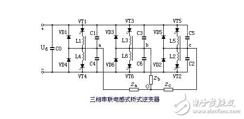
The three-phase series inductive inverter circuit is shown in the figure. In the figure, C0 is a DC filter capacitor, VT1 to VT6 are main thyristors, L1 to L6 are commutation inductors, C1 to C6 are commutation capacitors, and VD1 to VD6 are feedback diodes.
The inverter is of a 180° conduction type, and each thyristor is turned on by 180° in each cycle during a resistive load, and the interval between two trigger pulses of adjacent thyristors is 60°, and the commutation is in the same bridge arm. Intermittently, such as VT1 and VT4 of phase a, VT3 and VT6 of phase b, and VT5 and VT2 of phase c. One tube is turned on for each phase at any instant of each cycle. In order to ensure reliable commutation for large inductive loads, the trigger pulse width should be greater than 90°, typically 120°.

Characteristics
(1) The main thyristor is subjected to a low du/dt value.
(2) In addition to the load current, the main thyristor also bears the circulating current. When the output frequency of the inverter is high, the circulation is large, so it is not suitable for places with high frequency. In addition, the circulation is large and the commutation efficiency is low, so it is suitable for medium power loads.
(3) When the commutation parameter is constant and the load current is constant, the thyristor is subjected to the back pressure time with the DC voltage. ![]() It is reduced and reduced, so it is suitable for occasions where the voltage regulation range is not too large.
It is reduced and reduced, so it is suitable for occasions where the voltage regulation range is not too large.
Commutation process
The commutation between the thyristors is performed by forced commutation, which is accomplished by commutation capacitors and commutating inductors. Now let a phase VT1 commutate to VT4 as an example for general analysis.
When the thyristor VT1 is turned on, ![]() =0,
=0, ![]() =U, that is, the converter capacitor C4 is charged, so that the VT4 is subjected to the forward voltage and has a condition of conduction. When the VT4 is turned on, the capacitor C4 is discharged, and the discharge circuit is C4→L4→VT4.
=U, that is, the converter capacitor C4 is charged, so that the VT4 is subjected to the forward voltage and has a condition of conduction. When the VT4 is turned on, the capacitor C4 is discharged, and the discharge circuit is C4→L4→VT4. ![]() =
= ![]() . Since L4 and L1 are tightly coupled, the same voltage U is generated in L1, so that VT1 is subjected to back pressure and turned off. After VT1 is turned off, C1 is charged and C4 is discharged. At this time, the current corresponding to the original VT1 is turned on in L4.
. Since L4 and L1 are tightly coupled, the same voltage U is generated in L1, so that VT1 is subjected to back pressure and turned off. After VT1 is turned off, C1 is charged and C4 is discharged. At this time, the current corresponding to the original VT1 is turned on in L4. ![]() =
= ![]() In order to keep VT1 off, the magnetic energy in L1 is unchanged. The current in L4 is
In order to keep VT1 off, the magnetic energy in L1 is unchanged. The current in L4 is ![]() =L4
=L4 ![]() =L4
=L4 ![]() =0, the maximum value, after the current
=0, the maximum value, after the current ![]() =
= ![]() Falling, in L4, the potential of the opposite polarity is induced, so that VD4 is positively turned on and turned on, and VT4 is turned off. From the turn-on of VD4, the charging and discharging process of C1 and C4 is basically finished. After VD4 is turned on,
Falling, in L4, the potential of the opposite polarity is induced, so that VD4 is positively turned on and turned on, and VT4 is turned off. From the turn-on of VD4, the charging and discharging process of C1 and C4 is basically finished. After VD4 is turned on, ![]() The polarity is changed and the current remains in the original direction. Obviously this is determined by the nature of the inductive load. The length of the VD4 conduction time depends on the power factor angle of the load. But since the trigger pulse of VT4 does not disappear at this time, the current in VD4
The polarity is changed and the current remains in the original direction. Obviously this is determined by the nature of the inductive load. The length of the VD4 conduction time depends on the power factor angle of the load. But since the trigger pulse of VT4 does not disappear at this time, the current in VD4 ![]() After decreasing to zero, VT4 is turned back on. Therefore, VT4 undergoes a process of triggering conduction and ending to re-conduction. It should be pointed out that the initial process from turn-on to turn-off is very short, so it can be considered that when inductive load, when VT4 is triggered and VT1 is turned off, first, the feedback diode VD4 is turned on, and the time corresponding to the j angle is to be passed. After VT4 began to find.
After decreasing to zero, VT4 is turned back on. Therefore, VT4 undergoes a process of triggering conduction and ending to re-conduction. It should be pointed out that the initial process from turn-on to turn-off is very short, so it can be considered that when inductive load, when VT4 is triggered and VT1 is turned off, first, the feedback diode VD4 is turned on, and the time corresponding to the j angle is to be passed. After VT4 began to find.
Relationship between output voltage waveform and quantity of three-phase series inductive inverter
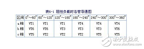
For resistive load, the continuity sequence of each tube is shown in Table 6-1.

During the period from 0° to 60°, VT1, VT6, and VT5 are turned on. Because the three-phase load is symmetrical, the phase voltage and line voltage are respectively
![]()
During the period of 60° to 120°, VT1, VT6, and VT2 are turned on. at this time
![]()
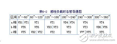
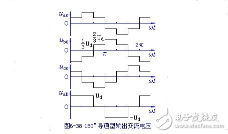
According to this analysis, the waveform of the phase voltage and line voltage of the load can be obtained as shown in Figure 6-38. For inductive loads, the continuity sequence of each tube is shown in Table 6-2.


As shown in Table 6-2, if the thyristors VT1 and VT4 of phase a are commutated (turning off VT1 and triggering VT4), the change in current direction in the inductive load lags behind the change in voltage polarity, so when VT1 is off After the disconnection, the freewheeling diode VD4, which is anti-parallel with VT4, should be turned on to ensure that the original current flow direction in the a phase is maintained after the voltage polarity is changed, and then the VT4 is turned on. It can be seen that the conduction angle of the thyristor in one cycle is q = 180°-j under inductive load. The total conduction angle of the thyristor and freewheeling diode is 180°. Regardless of the conduction voltage drop of the tube, VD4 or VT4 conduction does not affect the phase a voltage. Therefore, the output voltage waveform is the same as that of the resistive load, and the quantity relationship is the same. That is to say, the waveform and value of the AC output voltage of the 180° conduction type voltage inverter are independent of the load characteristics. At this time, the output voltage has a certain correspondence with the input voltage of the DC side. The advantages of the device.
Suizhou simi intelligent technology development co., LTD , https://www.msmvape.com