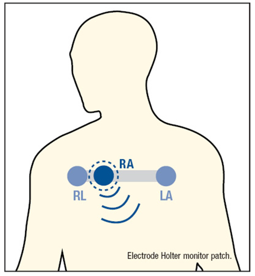
Traditional ECG monitors usually require a carry-on monitor to be placed close to the patient's neck or wrist pocket, and the noise and interference of the wireless ECG monitor is greatly reduced, and the size can be reduced to even the back of the electrode. Provides more accurate signals than traditional solutions. This circuit is inexpensive and provides a diagnostic quality 1 lead ECG trace that eliminates the need for a 60 Hz notch filter. All circuits can be worn in the clothes, so patient comfort and privacy are greatly improved.
The patient's monitoring data is encrypted and automatically uploaded to the on-site collection and analysis system in the hospital, nursing facility or maintenance facility every few minutes. The patient can upload information to the doctor's office or clinic at a predetermined time (daily or weekly) without removing the monitor or repositioning the electrodes. The wireless ECG monitor can also be equipped with a memory card for data transfer via a mobile phone or LAN. In addition to performance, reliability, low power consumption, and cost, the wireless ECG monitor design must support a dedicated telemetry band so that the monitor's ECG data can be quickly, accurately, and safely transmitted to the data collector for evaluation.
Overview
In North America, the Wireless Medical Telemetry Service (WMTS) band and other unlicensed industrial, scientific, and medical (ISM) bands provide dedicated spectrum to ensure uninterrupted, reliable connectivity for data transmission. ADI's ADF7021 high-performance, narrowband ISM transceiver IC supports the WMTS band and the ISM bands of 433 MHz, 868 MHz and 915 MHz. The ADF7021 offers best-in-class receiver sensitivity, -123 dBm at 1 kbps, built-in T/R switch, VCO tank, RF/IF filter, fully automated automatic frequency control (AFC) and automatic gain control (AGC) Circuit. To extend battery life, the ADF7021 can be placed in a very low power sleep mode, reducing current consumption to less than 0.1 μA. When used with a low-power microcontroller, the ADF7021 has an average standby current of less than 2 μA. The WMTS-optimized radio station reference design (EVAL-ADF7021DBZ6) includes schematics and layouts that can be used as a reference for wireless ECG monitor design.

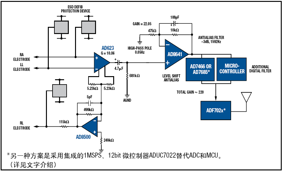
The wireless Holter monitor is extremely small enough to fit on the back of the ECG electrode, because it greatly reduces noise and interference, and its signal accuracy is superior to traditional designs. The circuit is inexpensive and provides a diagnostic-grade single-lead ECG. A 60 Hz notch filter is not required due to the presence of the drive legs. The transceiver (ADF702x shown below) and its peripheral circuitry vary with the frequency band in which it is used. Since all circuits can be worn in clothing, the patient's comfort and privacy are greatly enhanced.
Functional block diagram

The AD623 is an integrated single-supply instrumentation amplifier that provides rail-to-rail output swing and low power consumption (1.5 mW at 3 V). Its central node is used to access the residual common mode signal.
Details: AD623 Integrated Single Supply Instrumentation Amplifier
AD8500 low-power, high-precision current maximum power CMOS operational amplifier is 1 μA, the maximum offset voltage 1 mV, typical input offset current 1 pA, rail-to-rail input and output, a single 1.8 V ~ 5.5 V power supply or ± 0.9 V ~ ± 2.75 V dual supply.
Details: AD8500 Low Power, High Precision CMOS Operational Amplifier
The AD8641 low power, rail-to-rail output junction field effect transistor (JFET) amplifier features high input impedance, high precision performance, and low cost with an input impedance greater than 681 kΩ.
Details: AD8641 Low Power, Rail-to-Rail Output Junction Field Effect Transistor
The AD7466 is a 12-bit ADC in a small package with very low power consumption and consumes 480 μW at 3.6 V/50 kSPS. It is available in a 6-lead SOT-23 package. For a wider dynamic range and higher required SNR designs, AD7685 PulSAR® ADC can provide 16-bit resolution, at 2.5 V / 100 kSPS, power is 1.35 mW, which uses 3 mm & TImes; 3 Mm QFN (LFCSP) package.
Details: AD7466 12-bit ADC
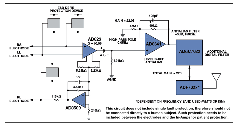
Another solution to achieve this signal chain is to replace the ADC and MCU with the ADuC7022. The functional block diagram is as follows. The ADuC7022 has a built-in 16-bit/32-bit MCU that integrates an ADC with performance up to 1 MSPS on a single chip. The ADC provides the necessary dynamic range to meet medical standards and detects weak ECG waveform changes. The ARM7 architecture includes a 32-bit register that enables real-time FIR filtering of ECG signals.
Functional block diagram

The ADuC70xx family is a fully integrated 1 MSPS, 12-bit data acquisition system that integrates a high-performance multi-channel ADC, 16-bit/32-bit MCU, and flash/EE memory in a single chip.
Details: ADuC7022: Precision Analog Microcontroller
Usb Docking Station,Usb Hub Docking Station,Docking Station With Hdmi,Usb C Hub Laptop Docking Station
Shenzhen GuanChen Electronics Co., Ltd. , https://www.gcneotech.com