With the popularity of computers, electronic pens have developed rapidly as emerging human-computer interaction tools. In China, Hanwang has always been a leader in handwriting recognition, leading the development of domestic electronic pens. In foreign countries, the handwriting is associated with office software, and the concept of digital ink is established. In June 2001, Ericsson announced the launch of the world's first digital pen, the Chat2penCHA-30. The product leverages Bluetooth wireless technology and a GPRS network to transmit handwritten text and interact with mobile phones, computers and the Internet. Although it looks and writes in the same way as a regular pen, Chatpen can "read" its position with a dot pattern that is almost invisible on plain paper. This information is transmitted via Bluetooth and GPRS mobile phones, allowing consumers to digitally write on paper at the same time. Users will find themselves no longer limited to text-based short messages or emails, as long as they use Chatpen to send handwritten notes at any time via a mobile phone, PC or PDA. Anything drawn or written down can be transmitted immediately, information processing becomes more personalized, and the process of sending text messages is greatly simplified by eliminating the need for alphanumeric input.
As the key technology behind the electronic pen, handwriting recognition has always been the focus of people's research. In general, the electronic pen can be divided into four categories according to different positioning methods: radio frequency positioning type, image recognition type, pressure sensing positioning type and acceleration positioning type. The radio frequency positioning type electronic pen needs to place an acoustic wave generator near the writing plane or on the writing board, and the ultrasonic wave generated by the generator completes the three-dimensional positioning of the brush stroke with high precision but complicated structure and algorithm. The image recognition type electronic pen applies an image recognition algorithm to recognize the handwriting image scanned by the miniature camera placed in the pen portion, and the handwriting is closest to the original track. The pressure-sensitive electronic pen needs a pressure-sensitive plate to feel the pressure of the pen tip and bend it into a recovery of the note. The accelerometer type electronic pen applies the kinematics algorithm, and obtains the movement track of the pen tip by calculating the acceleration, and combines the handwriting analysis algorithm to reproduce the handwriting, so the structure is simple and easy to implement. However, due to the resolution of the sensor, there is no such mature product on the market.
This solution uses Freescale Semiconductor's MMA7260Q three-axis low-level accelerometer to achieve spatial positioning of the stroke. Wireless USB devices provide a plug-and-play connection to the electronic pen. This electronic pen uses Cypress's 2.4GHz RF SoC CYRF6934 as the wireless USB network transceiver device. As long as the Cypress Encore2 wireless USB bridge is connected to the PC's USB port on the PC side, the electronic pen can perform one-way data to the PC. transmission.
1 Hardware planning
In this design, the MMA7260Q is used to measure the acceleration in the three axial directions of the electronic pens X, Y, and Z, so that the software can calculate the position of the pen tip in real time, thereby generating handwriting.
After the microcontroller ADuC7022 collects the signal output from the acceleration sensor, it uses the on-chip ADC to complete the conversion of the voltage signal to the acceleration data and performs signal processing. Finally, it is sent to the wireless USB interface chip CYRF6934 through the SPI interface, and the data is transmitted to the PC. Post processing.
The system is powered by a high-energy lithium battery. In order to achieve the longest possible battery life, all chips operate at 3.3V to reduce switching losses; after the microcontroller detects that the pen is stationary, the microcontroller software will put the wireless USB interface chip to sleep, further Reduce power consumption.
2 microcontroller circuit
The ADuC7022 is a new generation of analog analog microcontrollers based on the ARM7TDMI 32bit RISC core from ADI. It integrates a 10-channel 12-bit ADC (1MSPS), voltage comparator, 62Kbytes FlashROM and 8Kbytes SRAM on-chip with a maximum processing capacity of 40MIPS. Its analog peripherals include up to 10 channels of precision analog-to-digital converters (ADCs) with a sample rate of 1 MSPS and a resolution of 12 bits, and a precision bandgap reference with a temperature drift of better than 10ppm/°C. Other peripherals include on-chip programmable logic arrays (PLAs), synchronous, asynchronous serial interfaces, and more. Its on-chip PLL circuit allows the use of a lower frequency external crystal to reduce system EMI. The serial interface includes UART, SPI and 2 I2C, JTAG port for download/debug, 4 timers, 14 general purpose I/O pins. CPU clock up to 45MHz, on-chip crystal oscillator and on-chip PLL.
The ADuC7022 operates from 2.7V to 3.6V and consumes only 40mA at the maximum operating frequency of 41.78MHz. In addition, the ADuC702240 pin 6mm & TImes; 6mm LFCSP package can significantly reduce the board size, making it more suitable for most volume and power-consuming systems than most microcontrollers.
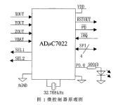
In this design, the ADuC7022 ADC operates in single-ended mode, ADC0~ADC2 of the ADC module is connected to the MMA7260Q triaxial acceleration output pin, ADC2 is connected to the positive battery, monitors the input battery voltage, and the battery voltage drops to near the LDO minimum input voltage. After the LED is lit, the user is prompted to replace the battery. The P0.0 and P0.1 pins of the microcontroller are connected to the SEL1 and SEL2 pins of the MMA7260Q as control signals for acceleration sensitivity.
The serial interface of the ADuC7022 provides SPI, UART, and I2C interfaces. The I/O port of the ADuC7022 is a multiplexed interface. The user can select among the GPIO, UART, UART/SPI/I2C and programmable logic array by setting the control register of the SPM module. This article uses a SPI module that works in Master mode and connects to a wireless USB module. The schematic of the microcontroller is shown in Figure 1.

3 acceleration sensor
The MMA7260Q is a single-chip, three-axis, low-magnification accelerometer from Freescale Semiconductor that accurately measures low-level drop, tilt, displacement, position, impact, and vibration errors in the X, Y, and Z directions. By choosing the sensitivity of the MMA7260Q, it is possible to design with gravitational acceleration sensitivities of different magnitudes (g) of 1.5g, 2g, 4g and 6g. The MA7260Q is fabricated using a MEMS process and integrates accelerometers and signal conditioning circuits such as low-pass filtering and temperature compensation in a 6mm & TImes; 6mm & TImes; 1.45mm volume, and presets a full-scale 0g offset. Its package size is small and requires less board space. In addition, the MMA7260Q can operate at a low voltage of 2.2V to 3.6V, and consumes only 500 during operation. It is equipped with a 3μA sleep mode and a 1.0ms fast power response. It also provides fast start and sleep modes. These features greatly extend the battery life of the electronic pen battery and leave enough space for the design.
SEL1 and SEL2 are sensitivity selection input pins, and the truth table of the corresponding sensitivity is shown in Table 1. The accelerometer output voltage VOUT is:


Among them, VOFFSET is 0 acceleration offset, ΔV/ΔG is acceleration sensitivity, 1G is earth gravity, and θ is tilt angle.
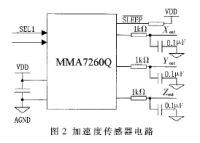
Xout, Yout and Zout are the output pins of the acceleration signals in the X, Y and Z directions respectively. The relationship between the output voltage and the acceleration is as shown in equation (1). The 0g bias voltage of the MMA7260Q is 1.65V. For a sensitivity of 1.5g, the output voltage per axis is between 0.85V and 2.45V.
The acceleration sensor circuit is shown in Figure 2. An RC filter is provided on the output of the MMA7260Q to filter out the interference of the internal switch filter capacitor clock and improve the measurement accuracy.

ZGAR Accessories
ZGAR electronic cigarette uses high-tech R&D, food grade disposable pod device and high-quality raw material. All package designs are Original IP. Our designer team is from Hong Kong. We have very high requirements for product quality, flavors taste and packaging design. The E-liquid is imported, materials are food grade, and assembly plant is medical-grade dust-free workshops.
Our products include disposable e-cigarettes, rechargeable e-cigarettes, rechargreable disposable vape pen, and various of flavors of cigarette cartridges. From 600puffs to 5000puffs, ZGAR bar Disposable offer high-tech R&D, E-cigarette improves battery capacity, We offer various of flavors and support customization. And printing designs can be customized. We have our own professional team and competitive quotations for any OEM or ODM works.
We supply OEM rechargeable disposable vape pen,OEM disposable electronic cigarette,ODM disposable vape pen,ODM disposable electronic cigarette,OEM/ODM vape pen e-cigarette,OEM/ODM atomizer device.

ZGAR Accessories Disposable Pod Vape,ZGAR Accessories Disposable Vape Pen,ZGAR Accessories,ZGAR Accessories Electronic Cigarette,ZGAR Accessories OEM vape pen,ZGAR Accessories OEM electronic cigarette.
Zgar International (M) SDN BHD , https://www.zgarecigarette.com